Download presentation
Presentation is loading. Please wait.

1
ALTERA UP2 Tutorial 1: The 15 Minute Design

2
Figure 1.1 The Altera UP 1 CPLD development board. ALTERA UP2 Tutorial 1: The 15 Minute Design

3
DesignCompilationSimulationVerifcation Graphical Entry HDL Entry Compiler Timing Diagram Timing Analysis Program CPLD UP 1 Development Board Figure 1.2 Design process for schematic or VHDL entry. ALTERA UP2 Tutorial 1: The 15 Minute Design

4
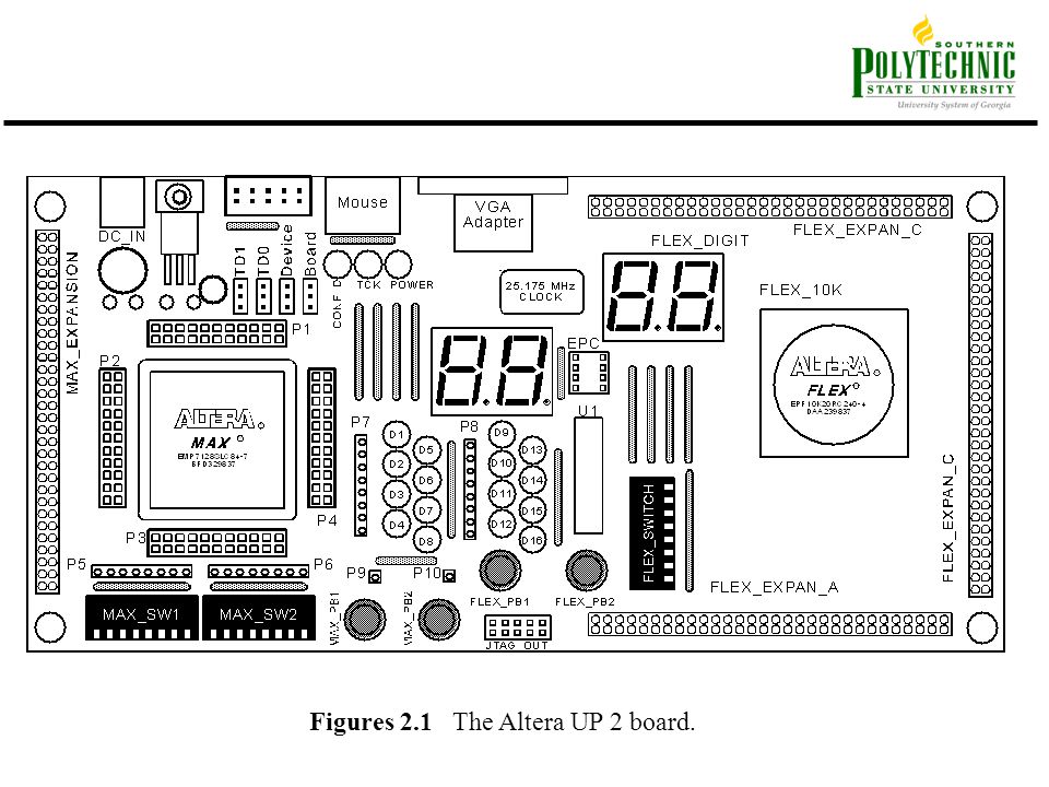
Figures 2.1 The Altera UP 2 board.

6
Table 2.1 UP 2 device selection jumpers for programming.

7
Figure 2.3 MAX and FLEX seven-segment LED display segment names.

8
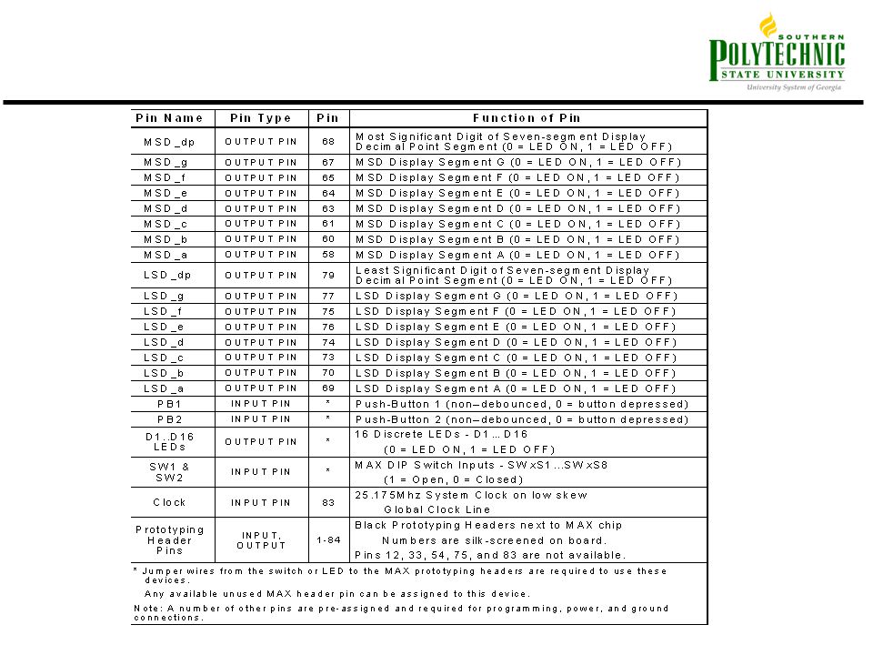
Table 2.4 UP 2 Board 10K20RC240 FLEX CHIP I/O pin assignments.

10
Figure 3.1 Digital logic technologies.

11
Figure 3.2 Digital logic technology tradeoffs.

12
Figure 3.3 Using a PLA to implement a Sum of Products equation.

13
Figure 3.4 Examples of FPLDs and advanced high pin count package types.

14
Figure 3.5 MAX 7000 macrocell. ALTERA MAX 7000 Architecture

15
Figure 3.6 MAX 7000 CPLD architecture. ALTERA MAX 7000 Architecture

16
Figure 3.7 FLEX 10K100 FPLD die photo, PIA interconnects are visible.

17
Figure 3.8 FLEX 10K Logic Element (LE).
.")
18
Figure 3.9 Using a lookup table (LUT) to model a gate network.
 to model a gate network.")
19
Figure 3.10 FLEX 10K Logic Array Block (LAB).
.")
20
Figure 3.11 FLEX 10K CPLD architecture.

21
Figure 3.12 Silicon wafer containing XC4010E 10,000 gate FPGAs. XILINX 4000 Architecture – A LU Table FPGA

22
Figure 3.13 Single XC4010E FPGA die showing 20 by 20 array of logic elements and interconnect. XILINX 4000 Architecture – A LU Table FPGA

23
Figure 3.14 Xilinx 4000 Family Configurable Logic Block (CLB).
.")
24
Figure 3.15 CAD tool design flow for Field Programmable Logic Devices (FPLDs).
.")
25
Figure 4.1 The tutor2.gdf schematic. Chapter 4: Tutorial II

26
Figure 4.2 8COUNT symbol online help file

27
Figure 4.3 Internal VHDL code for dec-7seg function.

28
Figure 4.4 Hierarchy display of the tutor2 design.

29
. Figure 4.5 Enlarged view of tutor2 design showing bus connections.

30
Figure 4.6 Timing analysis using Registered Performance option.

31
Figure 4.7 Oscilloscope display of pushbutton switch contact bounce.

32
Figure 4.8 Modified tutor2 design schematic.

Similar presentations


 COE 203 Digital Logic Laboratory Dr. Aiman El-Maleh College of Computer Sciences and Engineering.>")
 The slides included herein were taken.>")

 Fixed OR array programmable AND array Fixed OR array programmable AND array Easy to program Easy to program Poor flexibility.>")


>")


