Download presentation
Presentation is loading. Please wait.

1
By Squadron Leader Zahid Mir CS&IT Department, Superior University PHY-BE -02 Semiconductors

2
Semiconductors Materials whose electrical properties lies between those of insulators and conductors. – Have an almost empty conduction band and almost filled valance band with a narrow energy gap. – At 0 0 K there are no electrons in the conduction band and the valance band is completely filled. However with increase in temperature, width of forbidden energy band is decreased so that some electrons are liberated into the conduction band.

3
Atomic Binding in Semiconductors Tetravalent elements ; having 4 valance electrons. Form covalent bonds by sharing four electrons with each other so as to achieve inert gas structure. In case of pure semiconductor, the covalent bond has to be broken to provide electrons for conduction.

4
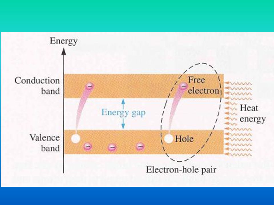
Hole Formation When an electron is ejected from the valance band, a covalent bond is broken and a positively charged hole is left behind.

6
Recombination Recombination occurs when a conduction electron loses energy and falls back into a hole in the valance band

7
Holes Flow Hole can travel to an adjacent atom by the acquiring an electron from the atom. Holes are filled up by electrons which moves from adjacent atoms without passing through the forbidden energy gap i.e conduction band has nothing to do with the hole flow.

9
Distinction between Holes & Electron Current Electron flow in conduction band whereas holes flow in valance band. Conduction electrons move almost twice as fast as the holes. The drift velocity of holes is obviously much less than the drift velocity of the conduction electrons.

10
Types of Semiconductors Intrinsic Semiconductors Extrinsic Semiconductors

11
Intrinsic Semiconductors Semiconductor in its pure form. Behaves like an insulator at 0 o K. Forbidden energy gap is of 0.72 – 1.1 eV (For Si & Ge respectively). Energy gap is so small that at even room temperature there are many electrons which possesses sufficient energy to jump across the energy gap into conduction band. For each liberated electron into the conduction band, a positively charged hole is created in the valance band.
. Energy gap is so small that at even room temperature there are many electrons which possesses sufficient energy to jump across the energy gap into conduction band. For each liberated electron into the conduction band, a positively charged hole is created in the valance band..")
12
Intrinsic Semiconductors When an electric field is applied to an intrinsic semiconductor at a temperature greater than 0 o K, conduction electrons move to the anode and the holes in the valance band to the cathode. Semiconductor current consists of movement of electrons & holes in opposite directions. Electrons current is due to movement of electrons in the conduction band whereas hole current is within the valance band as a result of holes “jumping” from one atom to another.

13
Effect of Temperature on Semiconductors An increase in temperature in conductors results in increase in resistance; hence conductors are said to have positive temperature coefficient. In semiconductors, on the other hand, an increase in temperature results in a substantial increase in the number of free electrons in the material. This increase of charge carriers increases the conductivity in semiconductors and result in a lower resistance. Semiconductors thus shows a reduction in resistance with increase in temperature and are said to have a negative temperature coefficient.

14
References “A Textbook of Electrical Engineering” by B L Theraja “Electronic Devices” by Thomas L. Floyd(7 th Edition)
.")
Similar presentations


 silicon – Doping – Carrier concentrations.>")


 Also:n 0 p 0 = n.>")


