Download presentation
Presentation is loading. Please wait.

1
Combinational Logic Chapter 4

2
4.1 Combinational Circuits
Logic circuits for digital system Combinational circuits the outputs are a function of the current inputs Sequential circuits contain memory elements the outputs are a function of the current inputs and the state of the memory elements the outputs also depend on past inputs

3
A combinational circuits
2n possible combinations of input values Specific functions Adders, subtractors, comparators, decoders, encoders, and multiplexers MSI circuits or standard cells Combinational Logic Circuit n input variables m output variables

4
4-2 Analysis Procedure A combinational circuit
make sure that it is combinational not sequential No feedback path derive its Boolean functions (truth table) design verification a verbal explanation of its function
 design verification. a verbal explanation of its function.")
5
A straight-forward procedure
F2 = AB+AC+BC T1 = A+B+C T2 = ABC T3 = F2'T1 F1 = T3+T2

6
F1 = T3+T2 = F2'T1+ABC. = (AB+AC+BC)'(A+B+C)+ABC
F1 = T3+T2 = F2'T1+ABC = (AB+AC+BC)'(A+B+C)+ABC = (A'+B')(A'+C')(B'+C')(A+B+C)+ABC = (A'+B'C')(AB'+AC'+BC'+B'C)+ABC = A'BC'+A'B'C+AB'C'+ABC A full-adder F1: the sum F2: the carry
 (A+B+C)+ABC = (A +B )(A +C )(B +C )(A+B+C)+ABC = (A +B C )(AB +AC +BC +B C)+ABC = A BC +A B C+AB C +ABC. A full-adder. F1: the sum. F2: the carry.")
7
The truth table

8
4-3 Design Procedure The design procedure of combinational circuits
State the problem (system spec.) determine the inputs and outputs the input and output variables are assigned symbols derive the truth table derive the simplified Boolean functions draw the logic diagram and verify the correctness
 determine the inputs and outputs. the input and output variables are assigned symbols. derive the truth table. derive the simplified Boolean functions. draw the logic diagram and verify the correctness.")
9
Functional description
Boolean function HDL (Hardware description language) Verilog HDL VHDL Schematic entry Logic minimization number of gates number of inputs to a gate propagation delay number of interconnection limitations of the driving capabilities
 Verilog HDL. VHDL. Schematic entry. Logic minimization. number of gates. number of inputs to a gate. propagation delay. number of interconnection. limitations of the driving capabilities.")
10
Code conversion example
BCD to excess-3 code The truth table

11
The maps

12
The simplified functions
z = D' y = CD +C'D' x = B'C + B'D+BC'D' w = A+BC+BD Another implementation z = D' y = CD +C'D' = CD + (C+D)' x = B'C + B'D+BC'D‘ = B'(C+D) +B(C+D)' w = A+BC+BD
 x = B C + B D+BC D‘ = B (C+D) +B(C+D) w = A+BC+BD.")
13
The logic diagram

14
4-4 Binary Adder-Subtractor
Half adder 0+0=0 ; 0+1=1 ; 1+0=1 ; 1+1=10 two input variables: x, y two output variables: C (carry), S (sum) truth table
, S (sum) truth table.")
15
S = x'y+xy' C = xy the flexibility for implementation S=xÅy S = (x+y)(x'+y') S' = xy+x'y' S = (C+x'y')' C = xy = (x'+y')'
")
17
Full-Adder The arithmetic sum of three input bits three input bits
x, y: two significant bits z: the carry bit from the previous lower significant bit Two output bits: C, S

19
S = x'y'z+x'yz'+ xy'z'+xyz C = xy + xz + yz
= z'xy'+z'x'y+z((x'+y)(x+y')) = z'(xy'+x'y)+z(xy'+x'y)' = zÅ (xÅy) C = xy'z+x'yz+xy =z(xy'+x'y)+xy =z(xÅy)+xy
(x+y )) = z (xy +x y)+z(xy +x y) = zÅ (xÅy) C = xy z+x yz+xy =z(xy +x y)+xy. =z(xÅy)+xy.")
20
Binary adder

21
Carry propagation when the correct outputs are available
the critical path counts (the worst case) (A1,B1,C1) > C2 > C3 > C4 > (C5,S4) > 8 gate levels
 (A1,B1,C1) > C2 > C3 > C4 > (C5,S4) > 8 gate levels.")
22
Reduce the carry propagation delay
employ faster gates look-ahead carry (more complex mechanism, yet faster) carry propagate: Pi = AiÅBi carry generate: Gi = AiBi sum: Si = PiÅCi carry: Ci+1 = Gi+PiCi C1 = G0+P0C0 C2 = G1+P1C1 = G1+P1(G0+P0C0) = G1+P1G0+P1P0C0 C3 = G2+P2C2 = G2+P2G1+P2P1G0+ P2P1P0C0
 carry propagate: Pi = AiÅBi. carry generate: Gi = AiBi. sum: Si = PiÅCi. carry: Ci+1 = Gi+PiCi. C1 = G0+P0C0. C2 = G1+P1C1 = G1+P1(G0+P0C0) = G1+P1G0+P1P0C0. C3 = G2+P2C2 = G2+P2G1+P2P1G0+ P2P1P0C0.")
23
Logic diagram

24
4-bit carry-look ahead adder
propagation delay

25
Binary subtractor A-B = A+(2’s complement of B) 4-bit Adder-subtractor
M=0, A+B; M=1, A+B’+1

26
Overflow The storage is limited
Add two positive numbers and obtain a negative number Add two negative numbers and obtain a positive number V=0, no overflow; V=1, overflow

27
4-5 Decimal Adder Add two BCD's Design approaches
9 inputs: two BCD's and one carry-in 5 outputs: one BCD and one carry-out Design approaches A truth table with 2^9 entries use binary full Adders the sum <= = 19 binary to BCD

28
The truth table

29
Modifications are needed if the sum > 9
C = K+ Z8Z4 + Z8Z2 C = 1 K = 1 Z8Z4 = 1 Z8Z2 = 1 modification: -(10)d or +6
d or +6.")
30
Block diagram

31
Binary Multiplier Partial products – AND operations

32
4-bit by 3-bit binary multiplier

33
4-7 Magnitude Comparator
The comparison of two numbers outputs: A>B, A=B, A<B Design Approaches the truth table 22n entries - too cumbersome for large n use inherent regularity of the problem reduce design efforts reduce human errors

34
Algorithm -> logic Implementation A = A3A2A1A0 ; B = B3B2B1B0
A=B if A3=B3, A2=B2, A1=B1and A1=B1 equality: xi= AiBi+Ai'Bi' (A=B) = x3x2x1x0 (A>B) = A3B3'+x3A2B2'+x3x2A1B1'+x3x2x1 A0B0' (A>B) = A3'B3+x3A2'B2+x3x2A1'B1+x3x2x1 A0'B0 Implementation xi = (AiBi'+Ai'Bi)'
 = x3x2x1x0. (A>B) = A3B3 +x3A2B2 +x3x2A1B1 +x3x2x1 A0B0 (A>B) = A3 B3+x3A2 B2+x3x2A1 B1+x3x2x1 A0 B0. Implementation. xi = (AiBi +Ai Bi)")
36
4-8 Decoder A n-to-m decoder
a binary code of n bits = 2n distinct information n input variables; up to 2n output lines only one output can be active (high) at any time
 at any time.")
37
An implementation

38
Combinational logic implementation
each output = a minterm use a decoder and an external OR gate to implement any Boolean function of n input variables

39
Demultiplexers a decoder with an enable input
receive information on a single line and transmits it on one of 2n possible output lines

40
Decoder/demultiplexers

41
Expansion two 3-to-8 decoder: a 4-to-16 deocder a 5-to-32 decoder?

42
Combination Logic Implementation
each output = a minterm use a decoder and an external OR gate to implement any Boolean function of n input variables A full-adder S(x,y,x)=S(1,2,4,7) C(x,y,z)= S(3,5,6,7)
=S(1,2,4,7) C(x,y,z)= S(3,5,6,7)")
43
two possible approaches using decoder
OR(minterms of F): k inputs NOR(minterms of F'): 2n - k inputs In general, it is not a practical implementation
: k inputs. NOR(minterms of F ): 2n - k inputs. In general, it is not a practical implementation.")
44
4-9 Encoders The inverse function of a decoder

45
An implementation limitations illegal input: e.g. D3=D6=1
the output = 111 (¹3 and ¹6)
")
46
Priority Encoder resolve the ambiguity of illegal inputs
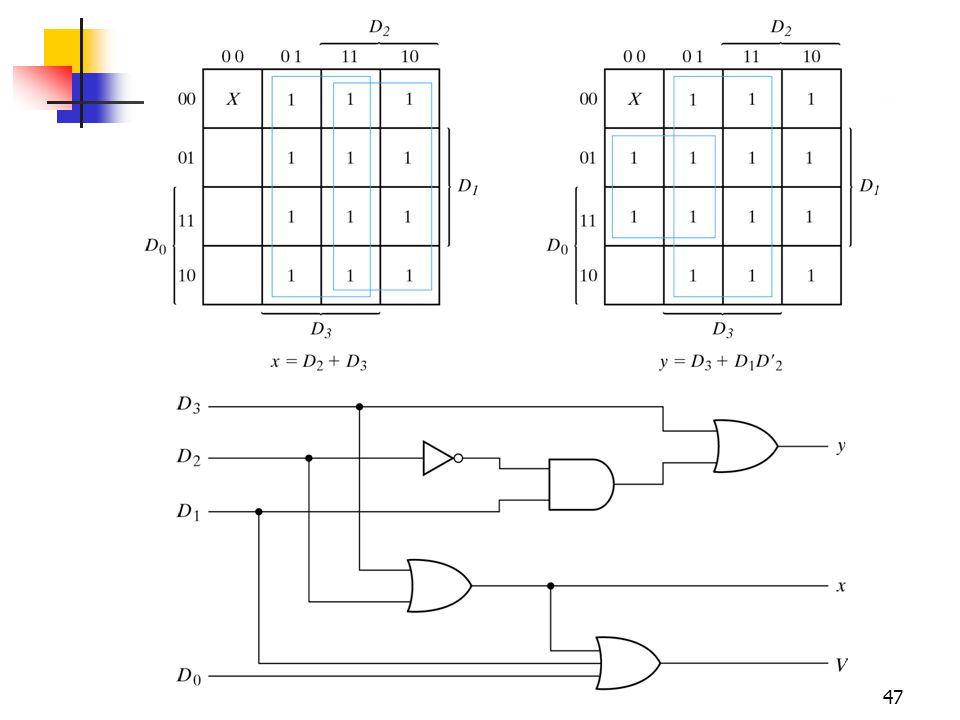
only one of the input is encoded D3 has the highest priority D0 has the lowest priority X: don't-care conditions V: valid output indicator

48
4-10 Multiplexers select binary information from one of many input lines and direct it to a single output line 2n input lines, n selection lines and one output line e.g.: 2-to-1-line multiplexer

49
4-to-1-line multiplexer

50
Note n-to- 2n decoder add the 2n input lines to each AND gate
OR(all AND gates) an enable input (an option)
 an enable input (an option)")
52
Boolean function implementation
MUX: a decoder + an OR gate 2n-to-1 MUX can implement any Boolean function of n input variable a better solution: implement any Boolean function of n+1 input variable n of these variables: the selection lines the remaining variable: the inputs

53
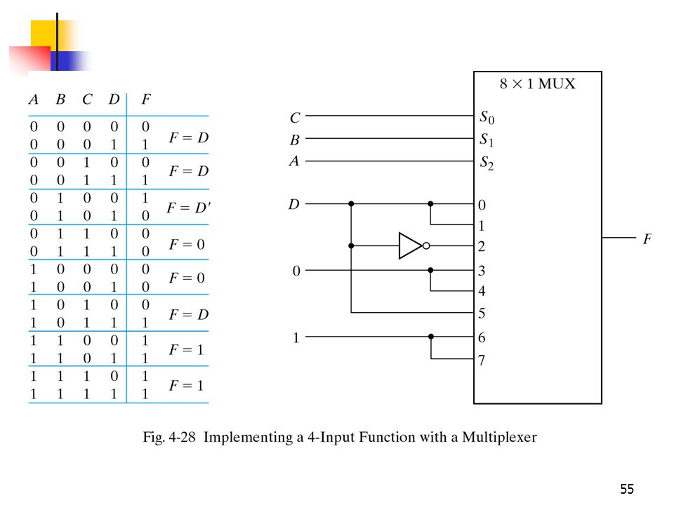
an example: F(A,B,C)=S(1,2,6,7)
=S(1,2,6,7)")
54
Procedure: assign an ordering sequence of the input variable
the rightmost variable (D) will be used for the input lines assign the remaining n-1 variables to the selection lines w.r.t. their corresponding sequence construct the truth table consider a pair of consecutive minterms starting from m0 determine the input lines
 will be used for the input lines. assign the remaining n-1 variables to the selection lines w.r.t. their corresponding sequence. construct the truth table. consider a pair of consecutive minterms starting from m0. determine the input lines.")
56
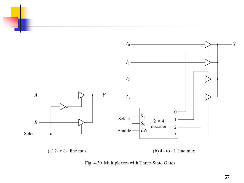
Three-state gates A multiplexer can be constructed with three-state gates Output state: 0, 1, and high-impedance (open ckts)
 .")
Similar presentations


 – –a fixed array of AND gates.>")


