Download presentation
Presentation is loading. Please wait.

1
Transducers Converts one type of energy into another.
Light Electrical (current, voltage, etc.) What characteristics should we look for in a transducer?
 What characteristics should we look for in a transducer")
2
Sensitivity and Responsivity
Responsivity, R(): Ratio of the signal output, x, to the incident radiant power, (in Watts). (voltage, current, charge) Sensitivity, Q(): Slope of a plot of x vs. . responsivity is evaluated at a particular wavelength and incident power sensitivity is slope of plot of electrical output (x) versus incident radiant power (phi) If Q is constant and independent of the incident radiant power (phi), the detector is said to exhibit linearity
: Ratio of the signal output, x, to the incident radiant power, (in Watts). (voltage, current, charge) Sensitivity, Q(): Slope of a plot of x vs. . responsivity is evaluated at a particular wavelength and incident power. sensitivity is slope of plot of electrical output (x) versus incident radiant power (phi) If Q is constant and independent of the incident radiant power (phi), the detector is said to exhibit linearity.")
3
Spectral Response Short l limit – determined by window material
A plot of Q vs lambda or R vs lambda is called the spectral response of the transducer Here, you see spectral response plots for several PMT models produced by Hamamatsu. You can see that the sensitivity varies significantly from wavelength to wavelength and model to model. The photocathode of a PMT converts the energy of incident photons into photoelectons. The conversion efficiency (photocathode sensitivity) varies with the incident wavelength of light. This relationship between the photocathode and the incident light wavelength is referred to as the spectral response characteristics. In general, the spectrla response characteristics are expressed in terms of radiant sensitivity and quantum efficiency. Short l limit – determined by window material Long l limit – determined by photocathode material Hamamatsu Catalogue
 varies with the incident wavelength of light. This relationship between the photocathode and the incident light wavelength is referred to as the spectral response characteristics. In general, the spectrla response characteristics are expressed in terms of radiant sensitivity and quantum efficiency. Short l limit – determined by window material. Long l limit – determined by photocathode material. Hamamatsu Catalogue.")
4
Transmittance of Window Materials
Hamamatsu Catalogue

5
Response Speed Consider a sinusoidal input into a transducer with a finite response time. If the frequency, fc, of the sinusoidal input is high, the transducer response cannot keep up. The frequency where R() drops to of the ideal is used to determine the time constant, . Detectors vary widely in their ability to detect rapid changes in incident radiant power. The response time is evaluated in terms of the time constant (tao) where fc is the frequence at which R(lambda) has fallen to of its maximum value when a sinusoidal input of frequency fc is incdent on the transduces.
 drops to of the ideal is used to determine the time constant, . Detectors vary widely in their ability to detect rapid changes in incident radiant power. The response time is evaluated in terms of the time constant (tao) where fc is the frequence at which R(lambda) has fallen to of its maximum value when a sinusoidal input of frequency fc is incdent on the transduces.")
6
Rise Time Time for the output to rise from 10% to 90% for an instantaneous increase in .

7
Dark Signal Output in the absence of input radiation.
Often limits S/N at low signal intensities. Dark signal can be due to different phenomena. photoemissive detectors exhibit dark signals due to theral emission of electrons dark current increases with increasing voltage but it is not necessarily linear sometimes hard to subtract out because of drift – can become major source of error Hamamatsu catalog

8
Vacuum Phototube (“Vacuum Photodiode”)
Photosensitive material: e.g. Cs3Sb, AgOCs One major application of the phototube was the reading of optical sound tracks for projected films. They were used in a variety of light-sensing applications until they were superseded by photoresistors and photodiodes. two electrodes sealed in an evacuated glass or silica envelope. Here you see a schematic of a phototube, its circuit symbol and a typical bias network. The photosensitive cathode can be made from a number of photoemissive materials. incoming photons strike a photocathode, generating electrons, which are attracted toward the anode. Thus current flow is dependent on the frequency and intensity of incoming light. Ingle and Crouch, Spectrochemical Analysis

9
Photoelectric Effect Photon must have some minimum energy to release an e-. Referred to as the work function. lt = hc/Ec = 1240/Ec For most metals the work function is ~2 – 5 eV. Upon exposing a metallic surface to electromagnetic radiation that is above the threshold frequency (which is specific to the type of surface and material), the photons are absorbed and current is produced. No electrons are emitted for radiation with a frequency below that of the threshold, as the electrons are unable to gain sufficient energy to overcome the electrostatic barrier presented by the termination of the crystalline surface (the material's work function). In 1905 it was known that the energy of the photoelectrons increased with increasing frequency of incident light, but the manner of the increase was not experimentally determined to be linear until 1915 when Robert Andrews Millikan showed that Einstein was correct.[2] By conservation of energy, the energy of the photon is absorbed by the electron and, if sufficient, the electron can escape from the material with a finite kinetic energy. A single photon can only eject a single electron, as the energy of one photon may only be absorbed by one electron. The electrons that are emitted are often termed photoelectrons. The photons of the light beam have a characteristic energy given by the wavelength of the light. In the photoemission process, if an electron absorbs the energy of one photon and has more energy than the work function, it is ejected from the material. If the photon energy is too low, however, the electron is unable to escape the surface of the material. Increasing the intensity of the light beam does not change the energy of the constituent photons, only their number, and thus the energy of the emitted electrons does not depend on the intensity of the incoming light. Electrons can absorb energy from photons when irradiated, but they follow an "all or nothing" principle. All of the energy from one photon must be absorbed and used to liberate one electron from atomic binding, or the energy is re-emitted. If the photon is absorbed, some of the energy is used to liberate it from the atom, and the rest contributes to the electron's kinetic (moving) energy as a free particle. The work function is the minimum energy (usually measured in electron volts) needed to remove an electron from a solid to a point immediately outside the solid surface. Here "immediately" means that the final electron position is far from the surface on the atomic scale but still close to the solid on the macroscopic scale. Work function is an important property of metal. The magnitude of work function is usually about a half of the ionization energy of a free atom of the metal. The threshold wavelength (lambda(t)) is related to the photochatode work function E(c) by this equation where lambda is in nm and E(c) is in eVs. The work function represents the energy which must be given to an electron in the Fermi level of a metal to raise it to the potential energy of the metal-vacuum interface. Douglas A. Skoog and James J. Leary, Principles of Instrumental Analysis, Saunders College Publishing, Fort Worth, 1992.
, the photons are absorbed and current is produced. No electrons are emitted for radiation with a frequency below that of the threshold, as the electrons are unable to gain sufficient energy to overcome the electrostatic barrier presented by the termination of the crystalline surface (the material s work function). In 1905 it was known that the energy of the photoelectrons increased with increasing frequency of incident light, but the manner of the increase was not experimentally determined to be linear until 1915 when Robert Andrews Millikan showed that Einstein was correct.[2] By conservation of energy, the energy of the photon is absorbed by the electron and, if sufficient, the electron can escape from the material with a finite kinetic energy. A single photon can only eject a single electron, as the energy of one photon may only be absorbed by one electron. The electrons that are emitted are often termed photoelectrons. The photons of the light beam have a characteristic energy given by the wavelength of the light. In the photoemission process, if an electron absorbs the energy of one photon and has more energy than the work function, it is ejected from the material. If the photon energy is too low, however, the electron is unable to escape the surface of the material. Increasing the intensity of the light beam does not change the energy of the constituent photons, only their number, and thus the energy of the emitted electrons does not depend on the intensity of the incoming light. Electrons can absorb energy from photons when irradiated, but they follow an all or nothing principle. All of the energy from one photon must be absorbed and used to liberate one electron from atomic binding, or the energy is re-emitted. If the photon is absorbed, some of the energy is used to liberate it from the atom, and the rest contributes to the electron s kinetic (moving) energy as a free particle. The work function is the minimum energy (usually measured in electron volts) needed to remove an electron from a solid to a point immediately outside the solid surface. Here immediately means that the final electron position is far from the surface on the atomic scale but still close to the solid on the macroscopic scale. Work function is an important property of metal. The magnitude of work function is usually about a half of the ionization energy of a free atom of the metal. The threshold wavelength (lambda(t)) is related to the photochatode work function E(c) by this equation where lambda is in nm and E(c) is in eVs. The work function represents the energy which must be given to an electron in the Fermi level of a metal to raise it to the potential energy of the metal-vacuum interface. Douglas A. Skoog and James J. Leary, Principles of Instrumental Analysis, Saunders College Publishing, Fort Worth,")
10
The Work Function Limits the Spectral Response
2-5 eV = nm Use materials with lower work functions, e.g., alkali metals. Hamamatsu Catalogue

11
Quantum Efficiency K()
# of photoelectrons ejected for every incident photon. Typically K() < 0.5 Rate of electrons emitted from the cathode (rcp): rcp = pK() where p is the photon flux (photons / sec). Multiply by electron charge to get current. icp = ercp = eK()p Only a certain fraction of the photons with greater than threshold energy yield photoelectrons with sufficient kinetic energy to escape the photocathode. This photoemission takes place according to a certain probability process. This fraction is called the quantum efficiency and is the ratio of the number of photoelectrons ejected to the number of incident photons Photons of shorter wavelengths carry higher energy compared to those of longer wavelength and contribute to an increase in the photoemission probability. As a result the maximum quantum efficiency occurs at a wavelength slightly shorter than the wavelength of peak radiant sensitivity. Often expressed as a percent Ingle and Crouch, Spectrochemical Analysis
 < 0.5. Rate of electrons emitted from the cathode (rcp): rcp = pK() where p is the photon flux (photons / sec). Multiply by electron charge to get current. icp = ercp = eK()p. Only a certain fraction of the photons with greater than threshold energy yield photoelectrons with sufficient kinetic energy to escape the photocathode. This photoemission takes place according to a certain probability process. This fraction is called the quantum efficiency and is the ratio of the number of photoelectrons ejected to the number of incident photons. Photons of shorter wavelengths carry higher energy compared to those of longer wavelength and contribute to an increase in the photoemission probability. As a result the maximum quantum efficiency occurs at a wavelength slightly shorter than the wavelength of peak radiant sensitivity. Often expressed as a percent. Ingle and Crouch, Spectrochemical Analysis.")
12
Radiant Cathodic Responsivity (R())
Efficiency with which photon energy is converted to photo-electrons. Units: A / W Values vary drastically for different kinds of detectors. As low as A/W for vacuum phototubes to A/W for photovoltaic cells Ingle and Crouch, Spectrochemical Analysis

13
Anodic Current Collection Efficiency () depends on the bias voltage (Eb). Arrival Rate at the Anode (collection rate): rap = rcp = pK() iap = icp = phR() p = photon flux Ingle and Crouch, Spectrochemical Analysis
: rap = rcp = pK() iap = icp = phR() p = photon flux. Ingle and Crouch, Spectrochemical Analysis.")
14
Are you getting the concept?
A vacuum phototube has radiant cathodic responsivity of 0.08 A/W at 400 nm. (a) Find the quantum efficiency at 400 nm. (b) If the incident photon flux at 400 nm is 2.75 x 10⁵ photons/sec, find the anodic pulse rate and the photoanodic current for a collection efficiency of 0.90. First, convert l to n → n = 7.5 x 10¹⁴ s-1 K(l) = R(l)hn/e = (0.08 As/J)(6.63 x Js)(7.5 x 10¹⁴ s-1) 1.602 x As K(l) = 0.248 rap = pK() = (0.90)(2.75 x 10⁵ photons/s)(0.248) rap = 6.15 x 10⁴ photons/s iap = phR() =(0.90)(2.75 x 10⁵ hn/s)(6.63 x Js)(7.5 x 10¹⁴ s-1)(0.08 As/J) iap = 9.7 x A Only a fraction of the photoelectrons emitted are collected at the anode. This fraction (eta) is called the collection efficiency, depends on the bias voltage (E(b)) and approaches unity if E(b)) is sufficiently high. The arrival rate of photoelectrons at the anode (r(ap)) and the anodic photocurrent (i(ap)) describe the effectiveness of photoelectron collection. Substitute in expressions for rate of electrons emitted from cathode (r(cp)) and current from cathode (i(cp))
 Find the quantum efficiency at 400 nm. (b) If the incident photon flux at 400 nm is 2.75 x 10⁵ photons/sec, find the anodic pulse rate and the photoanodic current for a collection efficiency of First, convert l to n → n = 7.5 x 10¹⁴ s-1. K(l) = R(l)hn/e = (0.08 As/J)(6.63 x Js)(7.5 x 10¹⁴ s-1) x As. K(l) = rap = pK() = (0.90)(2.75 x 10⁵ photons/s)(0.248) rap = 6.15 x 10⁴ photons/s. iap = phR() =(0.90)(2.75 x 10⁵ hn/s)(6.63 x Js)(7.5 x 10¹⁴ s-1)(0.08 As/J) iap = 9.7 x A. Only a fraction of the photoelectrons emitted are collected at the anode. This fraction (eta) is called the collection efficiency, depends on the bias voltage (E(b)) and approaches unity if E(b)) is sufficiently high. The arrival rate of photoelectrons at the anode (r(ap)) and the anodic photocurrent (i(ap)) describe the effectiveness of photoelectron collection. Substitute in expressions for rate of electrons emitted from cathode (r(cp)) and current from cathode (i(cp))")
15
Photomultiplier Tube m = k 8–19 dynodes (9-10 is most common).
Gain (m) is # e- emitted per incident e- () to the power of the # of dynodes (k). m = k E.g., 5 e- emitted / incident e-, 10 dynodes. Like a phototube, the PMT contains a photosensitive cathode and a collection anode. However, the cathode and anode are separated by several electrodes called dynodes that provide electron multiplication or gain. Unlike photomultiplier tubes, no amplification takes place, so the 'on' current is typically on the order of microamps. In a typical PMT, the cathode is biased negative by 400 – 2500 V wrt the anode. A photoelectron ejected byt the photocathode strikes the first dynode and releases two to five secondary electrons. Each electron is accelerated by the field between the first and second dynode and strike the next dynode with sufficient energy to release another two to five eletrons. Since each dynode down the chain is biased ~ 100 V more positive than the preceding dynode, this multiplication process ocntinues until the anode is reached. The rsult is a large charge packet of a few nanoseconds duration at the anode for each photoelectron collected by the first dynode. There are a variety of dynode types available and each exhibits a different gain, time response, uniformity, and secondary electron collection efficiency depending on structure and # of stages – here is the common “circular cage” arrangement m = k = 510 1 x 10⁷ Typical Gain = Douglas A. Skoog and James J. Leary, Principles of Instrumental Analysis, Saunders College Publishing, Fort Worth, 1992.
 is # e- emitted per incident e- () to the power of the # of dynodes (k). m = k. E.g., 5 e- emitted / incident e-, 10 dynodes. Like a phototube, the PMT contains a photosensitive cathode and a collection anode. However, the cathode and anode are separated by several electrodes called dynodes that provide electron multiplication or gain. Unlike photomultiplier tubes, no amplification takes place, so the on current is typically on the order of microamps. In a typical PMT, the cathode is biased negative by 400 – 2500 V wrt the anode. A photoelectron ejected byt the photocathode strikes the first dynode and releases two to five secondary electrons. Each electron is accelerated by the field between the first and second dynode and strike the next dynode with sufficient energy to release another two to five eletrons. Since each dynode down the chain is biased ~ 100 V more positive than the preceding dynode, this multiplication process ocntinues until the anode is reached. The rsult is a large charge packet of a few nanoseconds duration at the anode for each photoelectron collected by the first dynode. There are a variety of dynode types available and each exhibits a different gain, time response, uniformity, and secondary electron collection efficiency depending on structure and # of stages – here is the common circular cage arrangement. m = k = 510 1 x 10⁷. Typical Gain = Douglas A. Skoog and James J. Leary, Principles of Instrumental Analysis, Saunders College Publishing, Fort Worth,")
16
Choosing a PMT Average anodic current Single photon counting
most photocathodes are made of compound semiconductors which consist of alkali metals with a low work function. Each photocathode is available as a transmission type or a reflection type bialkali emply two kinds of alkali metals – give higher sensitivity than single alkali cathods luminous sensitivity – common way to evaluate the sensitivity… output current obtained from the cathode divided y the incident luminous flux (in lumens) from a tungsten lamp at a distribution temperature of 2856 K Average anodic current Single photon counting Hamamatsu Catalog
 from a tungsten lamp at a distribution temperature of 2856 K. Average anodic current. Single photon counting. Hamamatsu Catalog.")
17
Vacuum phototube iap = phR()
Anode Current iap = mphR() Remember: Vacuum phototube iap = phR()
 Remember: Vacuum phototube iap = phR()")
18
Modes of Operations Average anodic current Single photon counting
It is most common to measure the average current that results form the arrival of many anodic pulses. Here the electronics with a time constant much longer than the pulse duration are used to obtain the average photoanodic current i(ap) Alternatively, you can coung the number of anode pulses per unit time… Average anodic current Single photon counting Hamamatsu Catalog
 Alternatively, you can coung the number of anode pulses per unit time… Average anodic current. Single photon counting. Hamamatsu Catalog.")
19
Single Photon Counting
Single photons give bursts of e- The rise time of PMTs depends on the spread in the transit time of e- during the multiplication process. Called photon counting even though we’re actually counting packets of charge. PMTs are good for this because of the high gains… however, if the power supply is not stable, the gain (m) will change. Typically, the spread is about 10 ns but specially designed electron optics can reduce this time as seen here. FWHM: Full Width at Half of Maximum Hamamatsu Catalogue
 will change. Typically, the spread is about 10 ns but specially designed electron optics can reduce this time as seen here. FWHM: Full Width at Half of Maximum. Hamamatsu Catalogue.")
20
Single Photon Counting
Improved S/N at low p Have to discriminate between cosmic rays, signal, and dark current first then… At higher light levels, the output pulse intervals are narrow so that they overlap each other, producing (a) and (b) in bottom figure. If the light level becomes very low, the output signal will be discrete pulses… and photon counting is accomplished. Hamamatsu Catalogue
 and (b) in bottom figure. If the light level becomes very low, the output signal will be discrete pulses… and photon counting is accomplished. Hamamatsu Catalogue.")
21
Sources of Dark Current: Thermionic Emission
Thermal energy releases e- from the cathode. Reduced by cooling Thermionic emission (archaically known as the Edison effect) is the flow of electrons from a metal or metal oxide surface, caused by thermal vibrational energy overcoming the electrostatic forces holding electrons to the surface. The effect increases dramatically with increasing temperature (1000–3000 K). Because photocathode and dynodes have such low work functions, they emit thermionic electrons even at RT – the amount of thermionic emission is a function of the work function and the temperature When the work function is low, it extends the spectral range to higher wavelengths but increases thermionic emission (and thus, higher dark current). Hamamatsu Catalogue
 is the flow of electrons from a metal or metal oxide surface, caused by thermal vibrational energy overcoming the electrostatic forces holding electrons to the surface. The effect increases dramatically with increasing temperature (1000–3000 K). Because photocathode and dynodes have such low work functions, they emit thermionic electrons even at RT – the amount of thermionic emission is a function of the work function and the temperature. When the work function is low, it extends the spectral range to higher wavelengths but increases thermionic emission (and thus, higher dark current). Hamamatsu Catalogue.")
22
Thermionic Emission is Dependent on Bias Voltage
low voltage region (a) is dominated by the leakage current medium voltage region (b) is dominated by the thermionic emission high voltage region (c) is dominated by field emission and glass or electrode support scintillation Hamamatsu Catalogue
 is dominated by the leakage current. medium voltage region (b) is dominated by the thermionic emission. high voltage region (c) is dominated by field emission and glass or electrode support scintillation. Hamamatsu Catalogue.")
23
Sources of Dark Current: Ionization of Residual Gases
Ions formed when e- strike residual gas molecules. Gives a large noise spike when ion strikes cathode or one of the earlier dynodes. even though vacuum is 10-5 or 10-6 Torr, residual gases still exist in tube residual molecules may be ionized upon collision with electrons, when collide with cathode or dynodes, can trigger a cascade of electrons – dark signal

24
Sources of Dark Current: Glass Scintillation
Brief flash of light when an e- strikes the glass envelope. Douglas A. Skoog and James J. Leary, Principles of Instrumental Analysis, Saunders College Publishing, Fort Worth, 1992. some electrons will deviate from the expected trajectory and strike the glass housing – dark pulse Ingle and Crouch, Spectrochemical Analysis

25
Sources of Dark Current: Leakage Current (Ohmic Leakage)
Current from the glass base or the socket. Usually only significant at low bias. when the supply voltage is low and the PMT is cooled, the largest remaining contributor to dark current is the leakage current PMTs operate with high voltages but handle relatively small currents (microamperes) thus the insulating material in the PMT is very important. for instance, if the insulation material has a resistance of 10^12 ohms, the leakage current may reach the nanoampere level I(leakage current) = V (supply voltage)/R (insulator resistance) may be generated between anode and last dynode or at the glass base
 thus the insulating material in the PMT is very important. for instance, if the insulation material has a resistance of 10^12 ohms, the leakage current may reach the nanoampere level. I(leakage current) = V (supply voltage)/R (insulator resistance) may be generated between anode and last dynode or at the glass base.")
26
Photodiodes Photons incident on the depletion layer induce a current.
In most cases, best response in the NIR. Response is linear over 6 – 7 orders of incident radiant power Photodiodes are used in consumer electronics devices such as compact disc players, smoke detectors, and the receivers for remote controls in VCRs and televisions. In a photodiode, absorption of EM radiation by a pn junction diode causes promotion of electrons from the valence band to the conduction band and thus, the formation of electron-hole pairs in the depletion region (as illustrated) A photodiode is a p-n junction or p-i-n structure. When light with sufficient photon energy strikes a semiconductor, photons can be absorbed, resulting in generation of a mobile electron and electron hole. If the absorption occurs in the junction's depletion region, these carriers are swept from the junction by the built-in field of the depletion region, producing a photocurrent. The depletion region forms across the P-N junction when the junction is in thermal equilibrium, i.e. things are in a steady state. Electrons and holes will diffuse into regions with lower concentrations of electrons and holes, much as ink will diffuse into water until it is uniformly distributed throughout. N-type semiconductor has an excess of free electrons, and P-type has an excess of holes. Therefore when N-doped and P-doped pieces of semiconductor are placed together to form a junction, electrons will diffuse into the P side and holes will diffuse into the N side. However when a hole and an electron come into contact, they eliminate each other through recombination. This bares the donor atoms adjacent to the depletion region, which are now charged ions. The ions are positive on the N side and negative on the P side, creating an electric field that counteracts the continued diffusion of charge carriers. When the electric field is sufficient to repel incoming holes and electrons, the depletion region reaches its equilibrium width. Integrating the electric field in the depletion region gives what is known as the built-in potential (also called the junction voltage or barrier voltage). Under reverse bias (P negative with respect to N) this potential is increased, further widening the depletion zone. Forward bias (P positive with respect to N) narrows the zone and eventually reduces it to nothing, making the junction conductive and allowing free flow of charge carriers. The depletion region area is void of all majority carriers. Gain much lower than PMT but simplicity, excellent linearity, and small size make them attractive for applications where light levels are relatively hgih. Ingle and Crouch, Spectrochemical Analysis
 A photodiode is a p-n junction or p-i-n structure. When light with sufficient photon energy strikes a semiconductor, photons can be absorbed, resulting in generation of a mobile electron and electron hole. If the absorption occurs in the junction s depletion region, these carriers are swept from the junction by the built-in field of the depletion region, producing a photocurrent. The depletion region forms across the P-N junction when the junction is in thermal equilibrium, i.e. things are in a steady state. Electrons and holes will diffuse into regions with lower concentrations of electrons and holes, much as ink will diffuse into water until it is uniformly distributed throughout. N-type semiconductor has an excess of free electrons, and P-type has an excess of holes. Therefore when N-doped and P-doped pieces of semiconductor are placed together to form a junction, electrons will diffuse into the P side and holes will diffuse into the N side. However when a hole and an electron come into contact, they eliminate each other through recombination. This bares the donor atoms adjacent to the depletion region, which are now charged ions. The ions are positive on the N side and negative on the P side, creating an electric field that counteracts the continued diffusion of charge carriers. When the electric field is sufficient to repel incoming holes and electrons, the depletion region reaches its equilibrium width. Integrating the electric field in the depletion region gives what is known as the built-in potential (also called the junction voltage or barrier voltage). Under reverse bias (P negative with respect to N) this potential is increased, further widening the depletion zone. Forward bias (P positive with respect to N) narrows the zone and eventually reduces it to nothing, making the junction conductive and allowing free flow of charge carriers. The depletion region area is void of all majority carriers. Gain much lower than PMT but simplicity, excellent linearity, and small size make them attractive for applications where light levels are relatively hgih. Ingle and Crouch, Spectrochemical Analysis.")
27
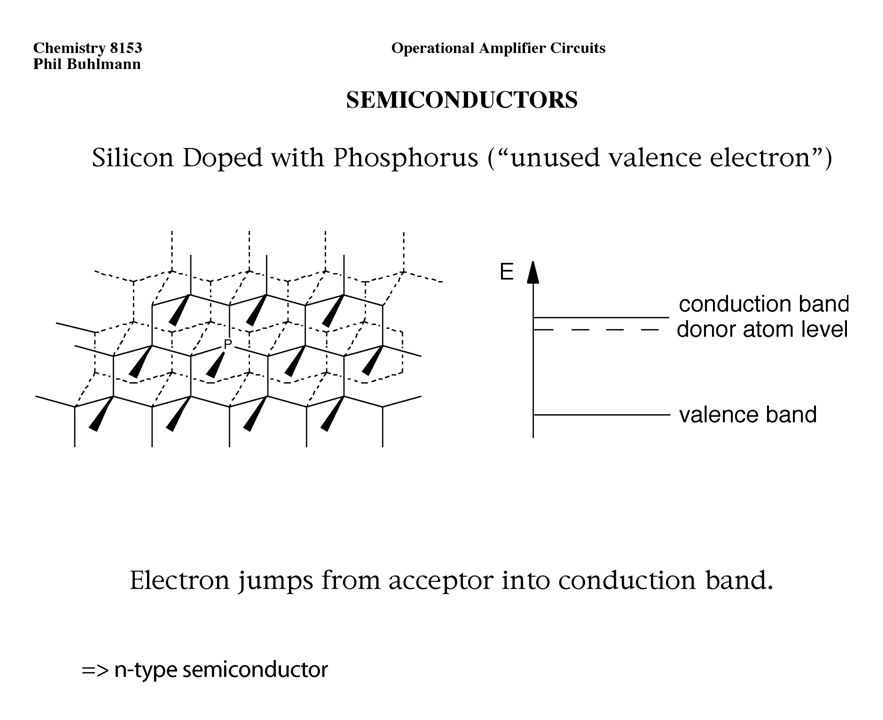
Semiconductors Silicon or Germanium are common.
n-type: Si (or Ge) doped with group V element (As, Sb) to add electrons. p-type: Doped with group III element (In, Ga) to add holes. J. Michael Hollas, Modern Spectroscopy, John Wiley & Sons, New York, 1992.
 doped with group V element (As, Sb) to add electrons. p-type: Doped with group III element (In, Ga) to add holes. J. Michael Hollas, Modern Spectroscopy, John Wiley & Sons, New York,")
30
Diode (pn – Junction) Douglas A. Skoog and James J. Leary, Principles of Instrumental Analysis, Saunders College Publishing, Fort Worth, 1992.

31
Photodiodes Photons incident on the depletion layer induce a current.
Cheap and Small. Ingle and Crouch, Spectrochemical Analysis

32
Spectral Response of Photodiodes
Comparison with photomultipliers Advantages compared to photomultipliers: Excellent linearity of output current as a function of incident light Spectral response from 190 nm to 1100 nm (silicon), longer wavelengths with other semiconductor materials Low noise Ruggedized to mechanical stress Low cost Compact and light weight Long lifetime High quantum efficiency, typically 80% No high voltage required Disadvantages compared to photomultipliers: Small area No internal gain (except avalanche photodiodes, but their gain is typically 102–103 compared to up to 108 for the photomultiplier) Much lower overall sensitivity Photon counting only possible with specially designed, usually cooled photodiodes, with special electronic circuits Response time for many designs is slower Shinya Inoue and Kenneth Spring, Video Microscopy, Plenum Press, New York, 1997.
, longer wavelengths with other semiconductor materials. Low noise. Ruggedized to mechanical stress. Low cost. Compact and light weight. Long lifetime. High quantum efficiency, typically 80% No high voltage required. Disadvantages compared to photomultipliers: Small area. No internal gain (except avalanche photodiodes, but their gain is typically 102–103 compared to up to 108 for the photomultiplier) Much lower overall sensitivity. Photon counting only possible with specially designed, usually cooled photodiodes, with special electronic circuits. Response time for many designs is slower. Shinya Inoue and Kenneth Spring, Video Microscopy, Plenum Press, New York,")
33
Avalanche Photodiode Hamamatsu Catalog
APDs are high-speed, high sensitivity photodiodes utilizing an internal gain mechanism that functions by applying a reverse voltage. When light enters a photodiode, electron-hole pairs are generated if the light energy is higher than the band gap energy. When electron-hole pairs are generated in the depletion layer of a photodiode with a reverse voltage applied to the pn junction, the electrons drift towards the N+ side while th eholes drift towards the P+ slide due to the electric field developed across the pn junction. The drift speed of these electron-hole pairs depends on the electric field strength. If the field is increased to a certain level, the electron-hole pairs are more likely to collide with the xtal lattice. If the reverse voltage is increased even further, some of the electron-hole pairs which escape collision with the xtal lattice will have a great deal of energy. When these electron-hole pairs finally do collide with the lattice, ionization will generate new electron-hole pairs… starting a chain reaction… avalanche multiplication of the photocurrent. The tutorial initializes with both the Photon Intensity and the Reverse Bias sliders set to an arbitrary mid-range value. Photons (yellow) entering the diode first pass through the silicon dioxide layer and then through the n and p layers before entering the depletion region where they excite free electrons (red) and holes (blue), which then migrate to the cathode and anode, respectively. Use the sliders to control the number of photons entering the diode and the reverse bias, which determines the number of electron/hole pairs generated by the photons. When a semiconductor diode has a reverse bias (voltage) applied and the crystal junction between the p and n layers is illuminated, then a current will flow in proportion to the number of photons incident upon the junction. Avalanche diodes are very similar in design to the silicon p-i-n diode, however the depletion layer in an avalanche photodiode is relatively thin, resulting in a very steep localized electrical field across the narrow junction. In operation, very high reverse-bias voltages (up to 2500 volts) are applied across the device. As the bias voltage is increased, electrons generated in the p layer continue to increase in energy as they undergo multiple collisions with the crystalline silicon lattice. This "avalanche" of electrons eventually results in electron multiplication that is analogous to the process occurring in one of the dynodes of a photomultiplier tube. Avalanche photodiodes are capable of modest gain ( ), but exhibit substantial dark current, which increases markedly as the bias voltage is increased (see Figure 1). They are compact and immune to magnetic fields, require low currents, are difficult to overload, and have a high quantum efficiency that can reach 90 percent. Avalanche photodiodes are now being used in place of photomultiplier tubes for many low-light-level applications.
 entering the diode first pass through the silicon dioxide layer and then through the n and p layers before entering the depletion region where they excite free electrons (red) and holes (blue), which then migrate to the cathode and anode, respectively. Use the sliders to control the number of photons entering the diode and the reverse bias, which determines the number of electron/hole pairs generated by the photons. When a semiconductor diode has a reverse bias (voltage) applied and the crystal junction between the p and n layers is illuminated, then a current will flow in proportion to the number of photons incident upon the junction. Avalanche diodes are very similar in design to the silicon p-i-n diode, however the depletion layer in an avalanche photodiode is relatively thin, resulting in a very steep localized electrical field across the narrow junction. In operation, very high reverse-bias voltages (up to 2500 volts) are applied across the device. As the bias voltage is increased, electrons generated in the p layer continue to increase in energy as they undergo multiple collisions with the crystalline silicon lattice. This avalanche of electrons eventually results in electron multiplication that is analogous to the process occurring in one of the dynodes of a photomultiplier tube. Avalanche photodiodes are capable of modest gain ( ), but exhibit substantial dark current, which increases markedly as the bias voltage is increased (see Figure 1). They are compact and immune to magnetic fields, require low currents, are difficult to overload, and have a high quantum efficiency that can reach 90 percent. Avalanche photodiodes are now being used in place of photomultiplier tubes for many low-light-level applications.")
34
Photodiode Arrays (PDA or DAD)
Simultaneous detection in a spectrophotometer. Arrays of silicon photodiodes… typically contain 256, 512, 1024 or 2048 elements arranged in a linear manner. Each diode in the array is sequentially interrogated… takes a few milliseconds Douglas A. Skoog and James J. Leary, Principles of Instrumental Analysis, Saunders College Publishing, Fort Worth, 1992.

35
Charge Coupled Device (CCD)
Charge-coupled devices (CCDs) are silicon-based integrated circuits consisting of a dense matrix of photodiodes that operate by converting light energy in the form of photons into an electronic charge. Electrons generated by the interaction of photons with silicon atoms are stored in a potential well and can subsequently be transferred across the chip through registers and output to an amplifier. The schematic diagram illustrated in Figure 1 shows various components that comprise the anatomy of a typical CCD. Advantages over traditional (PMT) detectors: Detects intensity with spatial resolution, Increased Sensitivity, Increased throughput due to lack of slits, More durable Disadvantages to traditional detectors: higher dark noise (important at low detection limits), Often requires liquid N2 cooling Most of the photons with a wavelength between 450 and 700 nanometers are absorbed either in the depletion region or within the bulk material (silicon) of a CCD substrate. Those absorbed into the depletion region will have a quantum efficiency approaching 100 percent, whereas photons entering the substrate liberate electrons that experience a three-dimensional random walk and either recombine with holes or diffuse into the depletion region. For those electrons that have negligible diffusion lengths, the quantum efficiency is very low, but those with high diffusion lengths eventually reach a charge well. Ingle and Crouch, Spectrochemical Analysis
 are silicon-based integrated circuits consisting of a dense matrix of photodiodes that operate by converting light energy in the form of photons into an electronic charge. Electrons generated by the interaction of photons with silicon atoms are stored in a potential well and can subsequently be transferred across the chip through registers and output to an amplifier. The schematic diagram illustrated in Figure 1 shows various components that comprise the anatomy of a typical CCD. Advantages over traditional (PMT) detectors: Detects intensity with spatial resolution, Increased Sensitivity, Increased throughput due to lack of slits, More durable. Disadvantages to traditional detectors: higher dark noise (important at low detection limits), Often requires liquid N2 cooling. Most of the photons with a wavelength between 450 and 700 nanometers are absorbed either in the depletion region or within the bulk material (silicon) of a CCD substrate. Those absorbed into the depletion region will have a quantum efficiency approaching 100 percent, whereas photons entering the substrate liberate electrons that experience a three-dimensional random walk and either recombine with holes or diffuse into the depletion region. For those electrons that have negligible diffusion lengths, the quantum efficiency is very low, but those with high diffusion lengths eventually reach a charge well. Ingle and Crouch, Spectrochemical Analysis.")
36
CCD Architecture Image Area SiO2 backing Pixel Array serial register
When a ultraviolet, visible, or infrared photon strikes a silicon atom resting in or near a CCD photodiode, it will usually produce a free electron and a "hole" created by the temporary absence of the electron in the silicon crystalline lattice. The free electron is then collected in a potential well (located deep within the silicon in an area known as the depletion layer), while the hole is forced away from the well and eventually is displaced into the silicon substrate. Individual photodiodes are isolated electrically from their neighbors by a channel stop, which is formed by diffusing boron ions through a mask into the p-type silicon substrate. The principal architectural feature of a CCD is a vast array of serial shift registers constructed with a vertically stacked conductive layer of doped polysilicon separated from a silicon semiconductor substrate by an insulating thin film of silicon dioxide (see Figure 2). After electrons have been collected within each photodiode of the array, a voltage potential is applied to the polysilicon electrode layers (termed gates) to change the electrostatic potential of the underlying silicon. The silicon substrate positioned directly beneath the gate electrode then becomes a potential well capable of collecting locally-generated electrons created by the incident light. Neighboring gates help to confine electrons within the potential well by forming zones of higher potentials, termed barriers, surrounding the well. By modulating the voltage applied to polysilicon gates, they can be biased to either form a potential well or a barrier to the integrated charge collected by the photodiode. serial register amplifier and Bryce Marquis (Haynes Lab)
![]()
37
Bryce Marquis (Haynes Lab)
CCD Architecture “Channel Stops” form horizontal pixel boundaries Top View 3 electrodes form vertical pixel boundaries One pixel The most common CCD designs have a series of gate elements that subdivide each pixel into thirds by three potential wells oriented in a horizontal row. Each photodiode potential well is capable of holding a number of electrons that determines the upper limit of the dynamic range of the CCD. After being illuminated by incoming photons during a period termed integration, potential wells in the CCD photodiode array become filled with electrons produced in the depletion layer of the silicon substrate. Measurement of this stored charge is accomplished by a combination of serial and parallel transfers of the accumulated charge to a single output node at the edge of the chip. The speed of parallel charge transfer is usually sufficient to be accomplished during the period of charge integration for the next image. After being collected in the potential wells, electrons are shifted in parallel, one row at a time, by a signal generated from the vertical shift register clock. The electrons are transferred across each photodiode in a multi-step process (ranging from two to four steps). This shift is accomplished by changing the potential of the holding well negative, while simultaneously increasing the bias of the next electrode to a positive value. The vertical shift register clock operates in cycles to change the voltages on alternate electrodes of the vertical gates in order to move the accumulated charge across the CCD. Figure 1 illustrates a photodiode potential well adjacent to a transfer gate positioned within a row of CCD gates. After traversing the array of parallel shift register gates, the charge eventually reaches a specialized row of gates known as the serial shift register. Here, the packets of electrons representing each pixel are shifted horizontally in sequence, under the control of a horizontal shift register clock, toward an output amplifier and off the chip. The entire contents of the horizontal shift register are transferred to the output node prior to being loaded with the next row of charge packets from the parallel register. In the output amplifier, electron packets register the amount of charge produced by successive photodiodes from left to right in a single row starting with the first row and proceeding to the last. This produces an analog raster scan of the photo-generated charge from the entire two-dimensional array of photodiode sensor elements. Once again every third electrode is in the serial register connected together. Below the image area (the area containing the horizontal electrodes) is the "Serial register". This also consists of a group of small surface electrodes. There are three electrodes for every column of the image area Electrode Insulating oxide n-type silicon p-type silicon Cross section Bryce Marquis (Haynes Lab)
. This shift is accomplished by changing the potential of the holding well negative, while simultaneously increasing the bias of the next electrode to a positive value. The vertical shift register clock operates in cycles to change the voltages on alternate electrodes of the vertical gates in order to move the accumulated charge across the CCD. Figure 1 illustrates a photodiode potential well adjacent to a transfer gate positioned within a row of CCD gates. After traversing the array of parallel shift register gates, the charge eventually reaches a specialized row of gates known as the serial shift register. Here, the packets of electrons representing each pixel are shifted horizontally in sequence, under the control of a horizontal shift register clock, toward an output amplifier and off the chip. The entire contents of the horizontal shift register are transferred to the output node prior to being loaded with the next row of charge packets from the parallel register. In the output amplifier, electron packets register the amount of charge produced by successive photodiodes from left to right in a single row starting with the first row and proceeding to the last. This produces an analog raster scan of the photo-generated charge from the entire two-dimensional array of photodiode sensor elements. Once again every third electrode is in the serial register connected together. Below the image area (the area containing the horizontal electrodes) is the Serial register . This also consists of a group of small surface electrodes. There are three electrodes for every column of the image area. Electrode. Insulating oxide. n-type silicon. p-type silicon. Cross section. Bryce Marquis (Haynes Lab)")
38
Charge Generation/Collection
-V +V -V -V +V -V N-type Photons entering the CCD create electron-hole pairs. The electrons are then attracted towards the most positive potential in the device where they create "charge packets". Each packet corresponds to one pixel. P-type Incident photons excite electron-hole pairs, electrons gather in potential wells in each pixel

39
CCD Rain Bucket Analogy
1. Generation 2. Collection 3. Transfer 4. Measurement the operation of a CCD is as follows: An number of buckets (Pixels) are distributed across a field (Focal Plane of a telescope) in a square array. The buckets are placed on top of a series of parallel conveyor belts and collect rain fall (Photons) across the field. The conveyor belts are initially stationary, while the rain slowly fills the buckets (During the course of the exposure). Once the rain stops (The camera shutter closes) the conveyor belts start turning and transfer the buckets of rain , one by one , to a measuring cylinder (Electronic Amplifier) at the corner of the field (at the corner of the CCD). Dump the first set of buckets into the special conveyor belt (the serial register) at the end of the array. Now, leave the ordinary conveyor belts fixed for a moment, and start to shift the special conveyor belt so that the first bucket empties into the graduated cylinder (readout amplifier). Record the amount of water (charge) in this first bucket, then shift the special conveyor belt again to bring the second bucket to the graduated cylinder. Record this bucket's contents, too, and then repeat until we've read all the buckets on the special conveyor belt. Shinya Inoue and Kenneth Spring, Video Microscopy, Plenum Press, New York, 1997.
 are distributed across a field (Focal Plane of a telescope) in a square array. The buckets are placed on top of a series of parallel conveyor belts and collect rain fall (Photons) across the field. The conveyor belts are initially stationary, while the rain slowly fills the buckets (During the course of the exposure). Once the rain stops (The camera shutter closes) the conveyor belts start turning and transfer the buckets of rain , one by one , to a measuring cylinder (Electronic Amplifier) at the corner of the field (at the corner of the CCD). Dump the first set of buckets into the special conveyor belt (the serial register) at the end of the array. Now, leave the ordinary conveyor belts fixed for a moment, and start to shift the special conveyor belt so that the first bucket empties into the graduated cylinder (readout amplifier). Record the amount of water (charge) in this first bucket, then shift the special conveyor belt again to bring the second bucket to the graduated cylinder. Record this bucket s contents, too, and then repeat until we ve read all the buckets on the special conveyor belt. Shinya Inoue and Kenneth Spring, Video Microscopy, Plenum Press, New York,")
40
Charge Generation/Collection
-V +V -V -V +V -V N-type silica is doped with pentavalent species = excess electrons P-type is doped with trivalent species = excess holes N-type Potential Well The n-type layer contains an excess of electrons that diffuse into the p-layer. The p-layer contains an excess of holes that diffuse into the n-layer. This structure is identical to that of a diode junction. The diffusion creates a charge imbalance and induces an internal electric field. The electric potential reaches a maximum just inside the n-layer, and it is here that any photo-generated electrons will collect. All science CCDs have this junction structure, known as a "Buried Channel". It has the advantage of keeping the photo-electrons confined away from the surface of the CCD where they could become trapped. It also reduces the amount of thermally generated noise (dark current). During integration of the image, one of the electrodes in each pixel is held at a positive potential. This further increases the potential in the silicon below that electrode and it is here that the photoelectrons are accumulated. The neighboring electrodes, with their lower potentials, act as potential barriers that define the vertical boundaries of the pixel. The horizontal boundaries are defined by the channel stops. P-type One Pixel
. During integration of the image, one of the electrodes in each pixel is held at a positive potential. This further increases the potential in the silicon below that electrode and it is here that the photoelectrons are accumulated. The neighboring electrodes, with their lower potentials, act as potential barriers that define the vertical boundaries of the pixel. The horizontal boundaries are defined by the channel stops. P-type. One Pixel.")
41
Charge Transfer Every third electrode is 2 coupled, charge packets
are walked towards Serial registry 2 +5V 0V -5V 1 +5V 0V -5V 3 to serial registry 1 In the following few slides, the implementation of the "conveyor belts" as actual electronic structures is explained. The charge is moved along these conveyor belts by modulating the voltages on the electrodes positioned on the surface of the CCD. The electrodes are grouped so that every third electrode shares the same voltage. Now, watch as the voltages supplied to the electrodes change, and the electron packets move in response. 2 3 Time-slice shown in diagram

42
+5V 0V -5V 2 +5V 0V -5V 1 +5V 0V -5V 3 1 2 3

43
+5V 0V -5V 2 +5V 0V -5V 1 +5V 0V -5V 3 1 2 3

44
+5V 0V -5V 2 +5V 0V -5V 1 +5V 0V -5V 3 1 2 3

45
+5V 0V -5V 2 +5V 0V -5V 1 +5V 0V -5V 3 1 At the end, we have moved all the charge packets over one pixel, and the voltages are back where they started. By repeating the sequence of voltage changes, we can move the packets another pixel down the column. 2 3

46
+5V 0V -5V 2 +5V 0V -5V 1 +5V 0V -5V 3 1 2 3

47
+5V 0V -5V 2 +5V 0V -5V 1 +5V 0V -5V 3 1 2 3

48
Charge Transportation
amplifier Pixels at end of the array dump charge into serial register Serial register walks charge packets to amplifier, where it is measured.

49
Quantum Efficiency www.piacton.com
The quantum efficiency of a charge-coupled device (CCD) is a property of the photovoltaic response defined as the number of electron-hole pairs created and successfully read out by the device for each incoming photon. This property is especially important for low-light imaging applications such as fluorescence microscopy where emission photon wavelengths are often in the nanometer range and have a relatively high absorption coefficient in silicon. Standard CCDs, which are illuminated in the front of the device through the gate electrodes and oxide coatings, are more sensitive to green and red wavelengths in the region between 550 and 900 nanometers. The spectral sensitivity of the CCD differs from that of a simple silicon photodiode detector because the CCD surface has channels used for charge transfer that are shielded by polysilicon gate electrodes, thin films of silicon dioxide, and a silicon nitride passivation layer. These structures, used to transfer the charge from the imaging area and to protect the CCD from humidity and electrostatic discharge, absorb the shorter wavelengths (450 nanometers and lower), reducing the blue sensitivity of the device. Polysilicon transmittance starts to decrease below 600 nanometers and the material becomes essentially opaque to photons at 400 nanometers, but absorption depends upon gate thickness and interference effects of light passing through thin films on the CCD surface. Interline-transfer CCDs have photodiodes that deviate from standard polysilicon gate structure, a factor that reduces interference effects and produces a more ideal and uniform spectral response. These devices are also usually equipped with vertical antibloom drains that produce a reduced response to longer wavelength photons. As photons above 700 nanometers penetrate deep into the silicon substrate close to the buried drain, they have a greater chance of liberating electrons that will diffuse into the drain and be instantly removed. Quantum efficiency is also dependent upon gate voltage, with lower voltages producing small depletion regions and visa versa.
 is a property of the photovoltaic response defined as the number of electron-hole pairs created and successfully read out by the device for each incoming photon. This property is especially important for low-light imaging applications such as fluorescence microscopy where emission photon wavelengths are often in the nanometer range and have a relatively high absorption coefficient in silicon. Standard CCDs, which are illuminated in the front of the device through the gate electrodes and oxide coatings, are more sensitive to green and red wavelengths in the region between 550 and 900 nanometers. The spectral sensitivity of the CCD differs from that of a simple silicon photodiode detector because the CCD surface has channels used for charge transfer that are shielded by polysilicon gate electrodes, thin films of silicon dioxide, and a silicon nitride passivation layer. These structures, used to transfer the charge from the imaging area and to protect the CCD from humidity and electrostatic discharge, absorb the shorter wavelengths (450 nanometers and lower), reducing the blue sensitivity of the device. Polysilicon transmittance starts to decrease below 600 nanometers and the material becomes essentially opaque to photons at 400 nanometers, but absorption depends upon gate thickness and interference effects of light passing through thin films on the CCD surface. Interline-transfer CCDs have photodiodes that deviate from standard polysilicon gate structure, a factor that reduces interference effects and produces a more ideal and uniform spectral response. These devices are also usually equipped with vertical antibloom drains that produce a reduced response to longer wavelength photons. As photons above 700 nanometers penetrate deep into the silicon substrate close to the buried drain, they have a greater chance of liberating electrons that will diffuse into the drain and be instantly removed. Quantum efficiency is also dependent upon gate voltage, with lower voltages producing small depletion regions and visa versa.")
50
Noise Sources in CCD Shot Noise Dark Signal Noise Readout Noise
Statistical variation of signal over time Increases with the square of the intensity Dark Signal Noise Caused by thermal liberation of electrons Strongly coupled to temperature Readout Noise Summation of noise associated with amplification of signal, and conversion from analogue to digital Increases with the processing speed

51
Other Issues: Bad Pixels
Increasing hot pixels Hot Pixels Increased charge accumulation due to variations in chip surface. Dead Pixels Defective pixels that do not respond.
![]()
52
Other Issues: Blooming
Saturation and blooming are related phenomena that occur in all charge-coupled device (CCD) image sensors under conditions in which either the finite charge capacity of individual photodiodes, or the maximum charge transfer capacity of the CCD, is reached. Once saturation occurs at a charge collection site, accumulation of additional photo-generated charge results in overflow, or blooming, of the excess electrons into adjacent device structures. A number of potentially undesirable effects of blooming may be reflected in the sensor output, ranging from white image streaks and erroneous pixel signal values (as illustrated in Figure 1) to complete breakdown at the output amplification stage, producing a dark image. The charge capacity of an image sensor can be limited by either the individual photodiode characteristics (pixels) or the CCD itself, and is defined by the maximum amount of charge that the image sensor can collect and transfer while still maintaining all of its design performance specifications. This capacity limit is termed the saturation charge level, and when this limit is reached, the pixel or CCD is described as being saturated. Exceeding the saturation level results in the generation of blooming artifacts in captured images. Blooming refers to the overflow of excess confined photo-generated charge from a photodiode well into adjacent structures when the maximum well charge capacity is exceeded. The extent of degradation of adjacent image areas as a result of blooming depends on the CCD fabrication details and the degree of charge overflow. Since the occurrence of blooming is triggered by the saturation condition, it is useful to know the detector output voltage corresponding to its maximum charge capacity. T
 image sensors under conditions in which either the finite charge capacity of individual photodiodes, or the maximum charge transfer capacity of the CCD, is reached. Once saturation occurs at a charge collection site, accumulation of additional photo-generated charge results in overflow, or blooming, of the excess electrons into adjacent device structures. A number of potentially undesirable effects of blooming may be reflected in the sensor output, ranging from white image streaks and erroneous pixel signal values (as illustrated in Figure 1) to complete breakdown at the output amplification stage, producing a dark image. The charge capacity of an image sensor can be limited by either the individual photodiode characteristics (pixels) or the CCD itself, and is defined by the maximum amount of charge that the image sensor can collect and transfer while still maintaining all of its design performance specifications. This capacity limit is termed the saturation charge level, and when this limit is reached, the pixel or CCD is described as being saturated. Exceeding the saturation level results in the generation of blooming artifacts in captured images. Blooming refers to the overflow of excess confined photo-generated charge from a photodiode well into adjacent structures when the maximum well charge capacity is exceeded. The extent of degradation of adjacent image areas as a result of blooming depends on the CCD fabrication details and the degree of charge overflow. Since the occurrence of blooming is triggered by the saturation condition, it is useful to know the detector output voltage corresponding to its maximum charge capacity. T.")
53
Other Issues: Cosmic Rays
Noise From Outer Space!!! * indicates cosmic rays

54
Other Issues: Etaloning
Advantage: S/N increases over a factor of 2 due to increased throughput Decreases shot noise Disadvantages: Decreased saturation limits Etaloning limits NIR detection

55
Other Features: Binning
On Chip Pixel Binning Increases S/N Shot noise decrease Increased speed Less storage space needed Decreases resolution Pixel binning is a clocking scheme used to combine the charge collected by several adjacent CCD pixels, and is designed to reduce noise and improve the signal-to-noise ratio and frame rate of digital cameras. The binning process is performed by on-chip CCD clock timing circuitry that assumes control of the serial and parallel shift registers prior to amplification of the CCD analog signal. To help illustrate the pixel binning process, refer to Figure 1, which reviews an example of 2 x 2 binning. A schematic drawing of a 4 x 4 parallel shift register pixel array is illustrated in Figure 1(a), along with a four-gate serial shift register and summing pixel or well (also termed an output node). Illuminating photons impact the CCD photodiodes, creating a pool of electrons that accumulates in each pixel, shown in Figure 1(b) as a cluster of four blue-shaded squares in the upper right hand corner of the parallel shift register. The number of electrons that each pixel can accommodate is termed the well depth and ranges from about 30,000 to 350,000, depending upon the CCD specifications. Dynamic range of a CCD is directly proportional to the well depth. Incident light levels and exposure time determine the number of electrons collected at each photogate or pixel site. After exposure of the CCD to one illumination cycle is completed, the electrons are transferred through the parallel and serial shift registers to a output amplifier and then digitized by an analog-to-digital (A/D) converter circuit. Binning can be used to increase focusing accuracy by reducing the time necessary for image acquisition, while providing greater sensitivity to lower out-of-focus light levels. To illustrate this process, Figure 1(b) shows each integrated pixel in the parallel register stepping by an increment of one gate to yield the arrangement shown in Figure 1(c). Here, the electrons from two pixels remain in the parallel shift register, while those from the other two have been transferred to the serial shift register. Another step (Figure 1(c)), shifts the remaining electrons in the parallel shift register to fill the adjacent gate elements in the serial register (Figure 1(d)). The final steps involve shifting of charge from the serial register, two pixels at a time, to the summing pixel (Figure 1(d) and (e)). Figure 1(f) illustrates the combined charge of four pixels in the summing well awaiting transfer to the output amplifier, where the signal will be converted to a voltage and then transferred to other integrated circuits for further amplification and digitization. The process continues until the entire array has been read out. In this example, the area of four adjacent pixels has been combined into one larger pixel, sometimes referred to as a super pixel. The signal-to-noise ratio has been increased by a factor of four, but the image resolution is cut by 50 percent.
, along with a four-gate serial shift register and summing pixel or well (also termed an output node). Illuminating photons impact the CCD photodiodes, creating a pool of electrons that accumulates in each pixel, shown in Figure 1(b) as a cluster of four blue-shaded squares in the upper right hand corner of the parallel shift register. The number of electrons that each pixel can accommodate is termed the well depth and ranges from about 30,000 to 350,000, depending upon the CCD specifications. Dynamic range of a CCD is directly proportional to the well depth. Incident light levels and exposure time determine the number of electrons collected at each photogate or pixel site. After exposure of the CCD to one illumination cycle is completed, the electrons are transferred through the parallel and serial shift registers to a output amplifier and then digitized by an analog-to-digital (A/D) converter circuit. Binning can be used to increase focusing accuracy by reducing the time necessary for image acquisition, while providing greater sensitivity to lower out-of-focus light levels. To illustrate this process, Figure 1(b) shows each integrated pixel in the parallel register stepping by an increment of one gate to yield the arrangement shown in Figure 1(c). Here, the electrons from two pixels remain in the parallel shift register, while those from the other two have been transferred to the serial shift register. Another step (Figure 1(c)), shifts the remaining electrons in the parallel shift register to fill the adjacent gate elements in the serial register (Figure 1(d)). The final steps involve shifting of charge from the serial register, two pixels at a time, to the summing pixel (Figure 1(d) and (e)). Figure 1(f) illustrates the combined charge of four pixels in the summing well awaiting transfer to the output amplifier, where the signal will be converted to a voltage and then transferred to other integrated circuits for further amplification and digitization. The process continues until the entire array has been read out. In this example, the area of four adjacent pixels has been combined into one larger pixel, sometimes referred to as a super pixel. The signal-to-noise ratio has been increased by a factor of four, but the image resolution is cut by 50 percent.")
Similar presentations


 Energy (J) Irradiance (W/m 2 ) Emittance (W/m 2 ) Intensity (W/sr) Radiance (W/sr m 2 )>")


>")


 Identify m of real source and adjust T in to line up m 2) The ratio of: 3) Measure T w ( ) to calculate ( ) Ingle and Crouch,>")
.>")


 What characteristics should we look for in a transducer?>")

