Download presentation
Presentation is loading. Please wait.

1
DRAM

3
Any read or write cycle starts with the falling edge of the RAS signal. –As a result the address applied in the address lines will be latched ( the row or high address). The signals on address lines will change to to represent the column or low address, which will be latched by the falling edge of the CAS signal. If OE is low the data will be gated to output data pins. If W is low the data will be latched from the data bus. DRAM timing
. The signals on address lines will change to to represent the column or low address, which will be latched by the falling edge of the CAS signal. If OE is low the data will be gated to output data pins. If W is low the data will be latched from the data bus. DRAM timing.")
4
Access time For DRAMs, there are three access times: –t RAC row access time: measured from falling edge of RAS to valid data out. –t CAC column access time: measured from falling edge of CAS to valid data out. –t AA address access time: measured from time of applying the address to valid data out.

5
FIGURE 7-50 Dynamic RAM timing. Two clock signals (RAS and CAS) are required to latch the multiplexed row and column addresses. Valid data appear tCAC ns after the clock goes low and remain until CAS returns high. John Uffenbeck The 80x86 Family: Design, Programming, and Interfacing, 3e Copyright ©2002 by Pearson Education, Inc. Upper Saddle River, New Jersey 07458 All rights reserved.
 are required to latch the multiplexed row and column addresses. Valid data appear tCAC ns after the clock goes low and remain until CAS returns high. John Uffenbeck The 80x86 Family: Design, Programming, and Interfacing, 3e Copyright ©2002 by Pearson Education, Inc. Upper Saddle River, New Jersey All rights reserved..")
6
In any read cycle, part of the memory cycle t RC time goes for pre-charging the bit since lines in preparation for the m emory cycle. (t PR and t CP ) data-out window= t RC -t CAC -t RP In fig 7-50 what is the width Valid data-out window? How it can be increased? –By keeping CAS low as necessary. –However this solution increases the cycle time. DRAM timing
 data-out window= t RC -t CAC -t RP In fig 7-50 what is the width Valid data-out window. How it can be increased. –By keeping CAS low as necessary. –However this solution increases the cycle time. DRAM timing.")
7
DRAM wait States DRAMs are characterized by the row access time. 60 ns DRAM means t RAC = 60 ns. How many wait states are needed by interfacing 60ns DRAM with a Pentium of 66 MHz external bus? processor accesses time is: 1.5/66MHz = 22.7 ns. the difference in access time is: 60 ns -22.7 ns =37.3 ns one wait state= 1/66MHz=15.2 ns required wait states =37.3/15.2=3 (check 22.7+(3*15.2)= 68.3 ns) BUT The whole memory cycle should end in 2T. 2T=30.3 ns, memory cycle time t RC = 110ns the difference in access time is: 110 ns -30.3 ns =79.7 ns required wait states = 79.7/15.2 = 6 wait states are required The Dram Cycle time is the limiting factor not the row access time
= 68.3 ns) BUT The whole memory cycle should end in 2T. 2T=30.3 ns, memory cycle time t RC = 110ns the difference in access time is: 110 ns ns =79.7 ns required wait states = 79.7/15.2 = 6 wait states are required The Dram Cycle time is the limiting factor not the row access time.")
8
Interleaving One way to improve the performance of of DRAM is INTERLEAVING. example: one bank stores 0-7,16-23, 32-39, etc.. the other bank stores 8-15, 24-31, 40-47 this to memory banks are said to be interleaved. In this way, the first bank is pre-charged while the second is being accessed. In this way the row access time is now, really, the access time.

9
advantage of interleaving (example) Consider the 60 ns DRAM with a Pentium of 66 MHz external bus. Calculate the transfer rate for: a) without interleaving b) with interleaving c) theoretical maximum (no wait states) a) 8*66/8 = 66 MB/s b) 8*66/5 = 105.6 MB/s c) 8*66/2=264 MB/s In this example interleaving increased the performance by about 50% However, even with interleaving, only 40% of the processor data transfer rate can be achieved.
 without interleaving b) with interleaving c) theoretical maximum (no wait states) a) 8*66/8 = 66 MB/s b) 8*66/5 = MB/s c) 8*66/2=264 MB/s In this example interleaving increased the performance by about 50% However, even with interleaving, only 40% of the processor data transfer rate can be achieved..")
10
FASTER DRAMs FPM, EDO, Synchronous (SDRAM) Fast Page Mode (FPM): FPM utilized the fact that usually read & write takes place in consecutive memory locations. after RAS clock falls low all the data in memory cells in the selected row are passed to the sense buffer. (this row is called page here) Now the CAS can be used to select memory locations in the selected row(page). Note that CAS is much faster than RAS.
 Now the CAS can be used to select memory locations in the selected row(page). Note that CAS is much faster than RAS..")
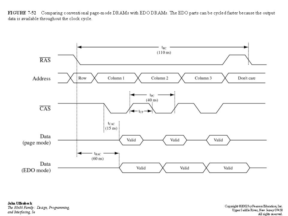
12
Extended Data Out DRAM –When CAS is high, Valid data remain in data pins. –This will increase the data-out window, without affecting the cycle time. –using page mode with EDO reduces the cycle time from 40ns( in none EDO) to 25ns. EDO DRAM
 to 25ns. EDO DRAM.")
13
Conventional DRAMs are asynchronous. After the memory address is applied to the chip, the data appears on the output pins some time later. Synchronous DRAM –control signals are applied on one clock rising edge. –and the data is transferred on a subsequent clock rising edge. –SDRAMs is designed to operate in Burst mode. they employ an onboard burst counter to generate the burst addresses ( the last three addresses.) –SDRAMs also employ interleaving which allows one internal memory bank to begin an access while another is finishing. SDRAM
 –SDRAMs also employ interleaving which allows one internal memory bank to begin an access while another is finishing. SDRAM.")
14
SDRAM example TMS626802 Clock frequency is 100 MHz. Two banks(B&T), 1MB each. each bank is 2K rows (11 lines) and 512 columns (9 lines). A11 is used to select the bank (0 for B, 1 for T). As usual RAS is used to strobe the row address (A0-A10), RAS is used to strobe the column address (A0-A8). It can be accessed in one-, two-,four-, eight-byte bursts. These bursts can be series or interleaved.
, 1MB each. each bank is 2K rows (11 lines) and 512 columns (9 lines). A11 is used to select the bank (0 for B, 1 for T). As usual RAS is used to strobe the row address (A0-A10), RAS is used to strobe the column address (A0-A8). It can be accessed in one-, two-,four-, eight-byte bursts. These bursts can be series or interleaved..")
15
FIGURE 7-54 The TMS626802 is organized as two separate 1M x 8 memory banks. (Courtesy of Texas Instruments.) John Uffenbeck The 80x86 Family: Design, Programming, and Interfacing, 3e Copyright ©2002 by Pearson Education, Inc. Upper Saddle River, New Jersey 07458 All rights reserved.
 John Uffenbeck The 80x86 Family: Design, Programming, and Interfacing, 3e Copyright ©2002 by Pearson Education, Inc. Upper Saddle River, New Jersey All rights reserved..")
16
FIGURE 7-55 Using column interleaving, the 626802 can access column addresses from two different row addresses. The access time is set by the clock period, which can be as short as 10 ns with the 100MHz part. (Courtesy of Texas Instruments.) John Uffenbeck The 80x86 Family: Design, Programming, and Interfacing, 3e Copyright ©2002 by Pearson Education, Inc. Upper Saddle River, New Jersey 07458 All rights reserved.
 John Uffenbeck The 80x86 Family: Design, Programming, and Interfacing, 3e Copyright ©2002 by Pearson Education, Inc. Upper Saddle River, New Jersey All rights reserved..")
17
Comparing RAMs Burst Timing

18
Refreshing DRAMs Each DRAM cell need to be refreshed. each cell should be refreshed once every few milliseconds (used to be 4ms). Can we refresh each cell (one at a time) in a 256 megabits DRAM: time to refresh a cell= 4ms/256Mbits=0.016ns – this is not enough to refresh a cell, and –No remaining time for useful read/write operations. Solution: select a row and refresh all the cells in that row.
. Can we refresh each cell (one at a time) in a 256 megabits DRAM: time to refresh a cell= 4ms/256Mbits=0.016ns – this is not enough to refresh a cell, and –No remaining time for useful read/write operations. Solution: select a row and refresh all the cells in that row..")
19
Refreshing DRAMs DRAMS used to have 256 rows each row should be refreshed every: 4ms/256= 15.6 s In other words, in order to refresh all the rows in 4ms, refresh cycle should be performed once every 15.6 s (which becomes the standard) New memories can have refresh period > 4ms. This implies DRAMS can have more rows. TMS417400 has 2048 rows: refresh period=2048* 15.6 s =32ms

20
Methods of Refreshing DRAMs RAS ONLY REFRESH To perform a RAS ONLY REFRESH, a row address is put on the address lines and then RAS is activated (goes low). As CAS is held HIGH, the Data pins will remain open. When RAS falls, that row will be refreshed. It is the DRAM controller’s function to provide the addresses to be refreshed and make sure that all rows are being refreshed in the appropriate amount of time. Because of that it is difficult to implement, and further complicate the memory controller.

21
Methods of Refreshing DRAMs CAS Before RAS Refresh (CBR): Generating the refresh address internally. CAS goes low then RAS goes low. Multiple RAS clocks (while CAS continues to be low) will cause sequential row address to be generated by the DRAM and refreshed. Self Refresh CAS then RAS goes low and both continue to be low ( no need for RAS clock) An on-board oscillator generate the refresh address automatically.
 will cause sequential row address to be generated by the DRAM and refreshed. Self Refresh CAS then RAS goes low and both continue to be low ( no need for RAS clock) An on-board oscillator generate the refresh address automatically..")
22
Distributing the Refresh Cycle BURST Refresh All the rows are refreshed in one burst. Processor is forced into wait state during refreshing, After refreshing all the rows, normal processing is resumed until the next refresh period. Question: Assume a RAS only refresh is used, and each cycle requires 110ns Calculate the time required to refresh the entire chip in one burst? 2048*110ns=225.28 s For what Percentage of refresh period is the DRAM accessible by the the processor? (32000-225.28)/32000 = 99.3% Note that:the refresh period is 32ms (2048*15.6 s)
/32000 = 99.3% Note that:the refresh period is 32ms (2048*15.6 s).")
23
Distributing the Refresh Cycle BURST Refresh All the rows are refreshed in one burst. Processor is forced into wait state during refreshing, After refreshing all the rows, normal processing is resumed until the next refresh period. Question: Assume a RAS only refresh is used, and each cycle requires 110ns Calculate the time required to refresh the entire chip in one burst? 2048*110ns=225.28 s For what Percentage of refresh period is the DRAM accessible by the the processor? (32000-225.28)/32000 = 99.3% Note that:the refresh period is 32ms (2048*15.6 s)
/32000 = 99.3% Note that:the refresh period is 32ms (2048*15.6 s).")
24
Distributing the Refresh Cycle Distributed Refresh Rather than refreshing the entire memory at once, The refresh cycles are distributed over the entire refresh period. A new refresh Cycle is generated every 15.6 s Most DRAM controllers use this technique. Question: If distributed refresh is used, calculate the number of instructions a 66 MHz processor can execute between refresh cycles? Assuming 1 instruction per clock cycle is executed. 1 clock cycle=1/66MHz=15ns Number of instructions=15625ns/15ns=2041 instruction.

25
Rambus Motivation: Looking to design a faster RAM SDRAM has: –12 to 16 address lines, 64 data line, 4 control lines –That means: – without good consideration of: the board layout, buss loading and termination, short cycle time (fast switching) may produce: –noise, ringing, crosstalk. looking to minimize the number of signal wires and reduce the signaling voltage levels. focusing on developing narrow data pathways but running at a very high speed.

26
RDRAM RDRAM is the result of a collaboration between Intel and a company called Rambus It is a totally new RAM architecture. The original (Base) design run at 600MHz(PC600). Concurrent RDRAM run at 700MHz (PC700). A Direct Rambus run at 800MHz (PC800).
 design run at 600MHz(PC600). Concurrent RDRAM run at 700MHz (PC700). A Direct Rambus run at 800MHz (PC800)..")
27
RDRAM The Direct RDRAM is designed to have a 400 MHz serial data path. The data path size is two bytes. This RDRAM is called called 800Mhz I/O rate and called PC800. The data path can transfer data every edge clock. From the above, the maximum transfer rate is: (2 bytes * 2cloke edges * 400MHz)= 1.6 GB/s
= 1.6 GB/s.")
29
Compared to SDRAM Totally different architecture. Totally different control signals. RDRAMs are mounted on circuit boards called RIMMs. RIMMS have 184 pins and require continuity modules in any empty socket. Which one has a better performance:

31
Quotes!! “..Problems with both the Rambus technology and Intel's chipset supporting it - the i820 - delayed DRDRAM's appearance until late 1999 - much later than had been originally planned..”. “..Some benchmarks show little, if any, performance advantage for initial RDRAM-based systems compared to SDRAM based systems..”. “... So there we have it. RDRAM is faster then DDR RAM in all the benchmarks we performed, but the differences were quite small and would be unnoticeable to most people …”.

32
Last Slide

Similar presentations


 DRAM Cell – The Hydraulic Analogy DRAM Block Diagram Types of DRAM.>")

 –Structure of diode ROM –Types of ROMs. –ROM with 2-Dimensional Decoding. –Using.>")


 Organization.>")

 Organization – contd.>")
 -- dynamic.>")

 Basic instructions for booting the computer and loading the operating system are stored in.>")
 :- -RAM is the place in a computer where the operating system, application programs & data in current use.>")
1 Memory. CSIT 301 (Blum)2 Types of DRAM Asynchronous –The processor timing and the memory timing (refreshing schedule) were independent.>")