Download presentation
Presentation is loading. Please wait.

1
ILC Instrumentation R&D at SCIPP ILCWS ‘08 University of Illinois at Chicago November 22 2008 Bruce Schumm Santa Cruz Institute for Particle Physics

2
Faculty/Senior Vitaliy Fadeyev Alex Grillo Bruce Schumm Collaborator Rich Partridge Undergrads Sean Crosby Jerome Carman Jared Newmiller Ryan Stagg The SCIPP/UCSC SiLC/SiD GROUP (Harwdare R&D Participants) Lead Engineer: Ned Spencer Technical Staff: Max Wilder, Forest Martinez-McKinney All participants are mostly working on other things (BaBar, ATLAS, biophysics…) Students: undergrad physics and/or engineering majors at UCSC
 Lead Engineer: Ned Spencer Technical Staff: Max Wilder, Forest Martinez-McKinney All participants are mostly working on other things (BaBar, ATLAS, biophysics…) Students: undergrad physics and/or engineering majors at UCSC")
3
Recent Areas of Inquiry ILC-Specific LSTFE front-end chip development SiD sensor testing Generic Charge division and longitudinal resolution Noise sources in high-resolution limit

4
1-3 s shaping time (LSTFE-I is ~1.2 s); analog measurement is Time-Over-Threshold Process: TSMC 0.25 m CMOS The LSTFE ASIC
; analog measurement is Time-Over-Threshold Process: TSMC 0.25 m CMOS The LSTFE ASIC")
5
1/4 mip 1 mip 128 mip Operating point threshold Readout threshold High gain advantageous for overall performance (channel matching)
")
6
Noise vs. Capacitance (at shape = 1.2 s) Measured dependence is roughly (noise in equivalent electrons) noise = 375 + 8.9*C with C in pF. Experience at 0.5 m had suggested that model noise parameters needed to be boosted by 20% or so; these results suggest 0.25 m model parameters are accurate Noise performance somewhat better than anticipated. Observed Expected 1 meter EQUIVALENT CAPACITANCE STUDY
 Measured dependence is roughly (noise in equivalent electrons) noise = *C with C in pF. Experience at 0.5 m had suggested that model noise parameters needed to be boosted by 20% or so; these results suggest 0.25 m model parameters are accurate Noise performance somewhat better than anticipated. Observed Expected 1 meter EQUIVALENT CAPACITANCE STUDY.")
7
LSTFE-II Prototype Additional “quiescent” feedback to improve power- cycling switch-on from 30 msec to 1 msec Improved environmental isolation Additional amplification stage to improve S/N, control of shaping time, and channel-to-channel matching Improved control of return-to-baseline for < 4 mip signals (time-over-threshold resolution) 128 Channels (256 comparators) read out at 3 MHz, multiplexed onto 8 LVDS outputs Testing underway by end of calendar year
 128 Channels (256 comparators) read out at 3 MHz, multiplexed onto 8 LVDS outputs Testing underway by end of calendar year")
8
SiD Sensor Testing SiD 10cm x 10cm “tile” intended for “KPIX” kilo-channel bump-bond ASIC. Resistance from strips as well as traces. First look by SCIPP (Sean Crosby) Also looked at “charge division” sensor; want to read out 600 k implant at both ends; confirmed strip that shorts implant (268 ) mistakenly added by manufacturer. (Would like to savage one to measure implant resistance)
 Also looked at charge division sensor; want to read out 600 k implant at both ends; confirmed strip that shorts implant (268 ) mistakenly added by manufacturer. (Would like to savage one to measure implant resistance).")
9
Sensors bias at ~50 V. Capacitance shown is for all 1840 strips, but strips to backplane only SiD Tiles: Biasing and Plane-to-Plane Capacitance For now: single sensor (sensor #26)
.")
10
SiD Leakage Current (sensor #26): Average leakage for 1840 channels is about ~160 pA/channel Measured strip and trace resistances for two sensors: Sensor Number Strip Res.Typical Trace Res. 24578225 26511161 Looks a bit odd (just first blush still…)
.")
11
Longitudinal Resolution via Charge Division Proposed by Rich Partridge, based on seminal paper by Radeka: V. Radeka "Signal, Noise and Resolution in Position-Sensitive Detectors", IEEE Trans. Nucl. Sci. 21, 51 (1974), which in turn references earlier work with planar sensors from R.B. Owen and M.L. Awcock, IEEE Trans. Nucl. Sci. 15, 290 (1968) Small ($16K) LCRD grant supports this work. Progress due to UCSC undergraduate physics major Jerome Carman Basic idea: For resistive sensor, impedances dominated by sensor rather than amplifier input impedance charge should divide proportional to point of deposition. So, forget about metal strip and read out implant (~100k )
, which in turn references earlier work with planar sensors from R.B. Owen and M.L. Awcock, IEEE Trans. Nucl. Sci. 15, 290 (1968) Small ($16K) LCRD grant supports this work. Progress due to UCSC undergraduate physics major Jerome Carman Basic idea: For resistive sensor, impedances dominated by sensor rather than amplifier input impedance charge should divide proportional to point of deposition. So, forget about metal strip and read out implant (~100k ).")
12
Charge Division Sensor Mock-Up 10-stage RC network PC board (Jerome Carman)
")
13
Amplifiers: First Stage: TI OPA657 Low-noise FET OpAmp Later Stages: Analog Devices ADA4851 rail-to-rail video amp Charge Division Sensor Mock-Up Model 600 k resistive implant with 10-stage RC network Read out at both left (“L”) and right (“R”) ends
 and right ( R ) ends")
14
Readout Noise Results Try several configurations, looking at noise from RH amp Nominal 0.64 fC Short RH amp input (163 to ground) 0.26 fC Disconnect LH amp and short that end to ground 0.66 fC Disconnect LH amp and float that end 0.44 fC
 0.26 fC Disconnect LH amp and short that end to ground 0.66 fC Disconnect LH amp and float that end 0.44 fC")
15
Correlation Between Left and Right Readout Naïve expectation: Dominated by Johnson noise across resistive implant Noise should be anticorrelated Bad for position resolution Result: Observed correlation (3%) consistent with 0. Good news, but why?

16
Correlation Between Left and Right Readout Cont’d Replace network with single 600 k resistor Anticorrelation observed Network effects appear to de-cohere Johnson noise currents

19
Longitudinal Resolution Estimate Trying to measure fractional distance f from right to left end of strip: Rewrite: Then, and dL, dR apparently uncorrelated.

20
Longitudinal Resolution Estimate: Conclusion Depends upon location of hit (middle or near end of resistive implant) and the magnitude of the charge deposition. Assume a 4 fC deposition in the middle of the strip (x=1): However, note that, so this is not much better. Optimize shaping time, implant resistivity, ? Goal of better than 0.1 (1cm for SiD sensors).
: However, note that, so this is not much better. Optimize shaping time, implant resistivity, . Goal of better than 0.1 (1cm for SiD sensors)..")
21
Readout Noise for Linear Collider Applications Use of silicon strip sensors at the ILC tend towards different limits than for hadron collider or astrophysical applications: Long shaping time Resistive strips (narrow and/or long) But must also achieve lowest possible noise to meet ILC resolution goals. How well do we understand Si strip readout noise?

22
Standard Form for Readout Noise (Spieler) Series Resistance Amplifier Noise (series) Amplifier Noise (parallel) Parallel Resistance F i and F v are signal shape parameters that can be determined from average scope traces.
 Series Resistance Amplifier Noise (series) Amplifier Noise (parallel) Parallel Resistance F i and F v are signal shape parameters that can be determined from average scope traces.")
23
LONG LADDER CONSTRUCTION

24
Measured Noise vs. Sum of Estimated Contributions 72 cm Ladder Estimated Johnson noise for actual 65 m strip (part of estimate) Projected Johnson noise for 20 m strip (not part of estimate) Measured noise Sum of estimates 143 cm Ladder Noise calculation assuming 20 m strip width (actual is 60 m)
 Projected Johnson noise for 20 m strip (not part of estimate) Measured noise Sum of estimates 143 cm Ladder Noise calculation assuming 20 m strip width (actual is 60 m).")
25
Strip Noise Idea: “Center Tapping” – half the capacitance, half the resistance? Result: no significant change in measured noise However, sensors have 237 m pitch Currently characterizing CDF L00 sensors Measured noise Expected noise, assuming 75% reduction in strip noise

26
CDF L00 Sensor “Snake” CDF L00 strips: 310 Ohms per 7.75cm strip (~3x GLAST) Long-ladder readout noise dominated by series noise (?) Construct ladder by bonding strips together in “snake” pattern (Sean Crosby) At long shaping-time, bias resistors introduce dominant parallel noise contribution Sever and replace with custom biasing structure (significant challenge…) Thanks to Sean Crosby, UCSC undergraduate thesis student
 Long-ladder readout noise dominated by series noise ( ) Construct ladder by bonding strips together in snake pattern (Sean Crosby) At long shaping-time, bias resistors introduce dominant parallel noise contribution Sever and replace with custom biasing structure (significant challenge…) Thanks to Sean Crosby, UCSC undergraduate thesis student")
28
CDF L00 Sensor “Snake” CDF L00 “Snake” LSTFE1 chip on Readout Board

29
CDF L00 Sensor “Snake” CDF L00 “Snake” LSTFE1 chip on Readout Board

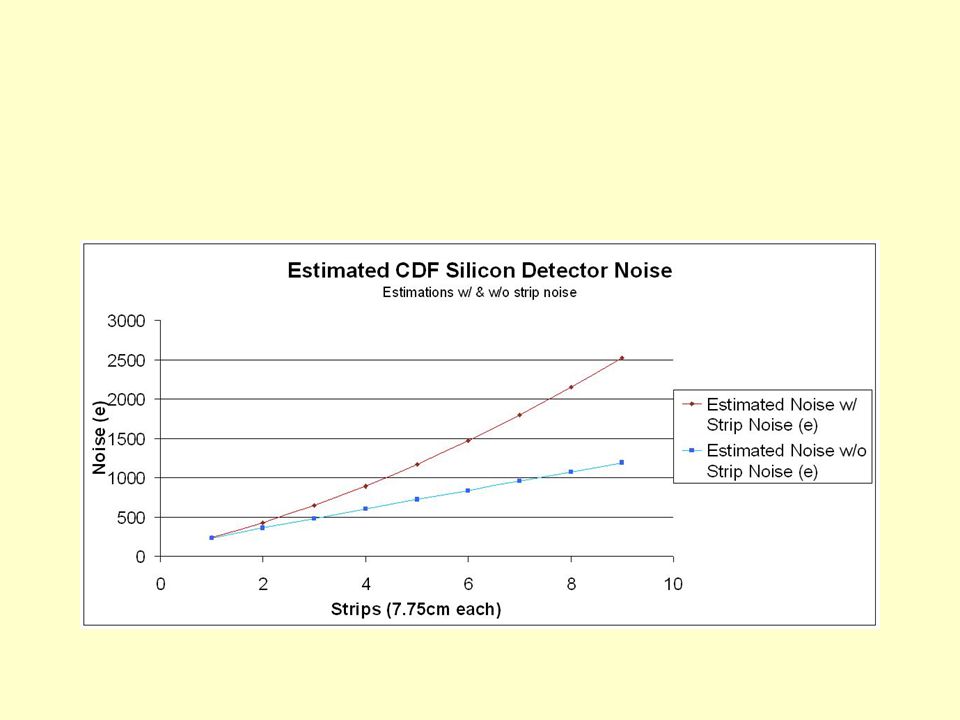
30
(After lengthy effort to eliminate non- fundamental noise sources) What happens when we add more CDF modules? Can we understand “extra” CDF noise by studying shaping-time dependence? Strip noise contribution should be negligible Strip noise should dominate after ~5 sensor lengths

31
Conclusions

Similar presentations


 CRYODET Workshop LNGS, 13-14 March 2006.>")


 Proposal Activities Radiation Hardness for BeamCal sensors (new; with SLAC) KPiX/Double Metal Performance.>")


