Download presentation
Presentation is loading. Please wait.

1
Activity 1 : Introduction to CCDs.
Simon Tulloch In this activity the basic principles of CCD Imaging is explained.

3
What is a CCD ? Charge Coupled Devices (CCDs) were invented in the 1970s and originally found application as memory devices. Their light sensitive properties were quickly exploited for imaging applications and they produced a major revolution in Astronomy. They improved the light gathering power of telescopes by almost two orders of magnitude. Nowadays an amateur astronomer with a CCD camera and a 15 cm telescope can collect as much light as an astronomer of the 1960s equipped with a photographic plate and a 1m telescope. CCDs work by converting light into a pattern of electronic charge in a silicon chip. This pattern of charge is converted into a video waveform, digitised and stored as an image file on a computer.

4
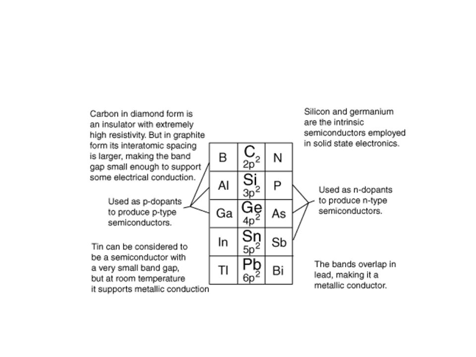
Photoelectric Effect. The effect is fundamental to the operation of a CCD. Atoms in a silicon crystal have electrons arranged in discrete energy bands. The lower energy band is called the Valence Band, the upper band is the Conduction Band. Most of the electrons occupy the Valence band but can be excited into the conduction band by heating or by the absorption of a photon. The energy required for this transition is 1.26 electron volts. Once in this conduction band the electron is free to move about in the lattice of the silicon crystal. It leaves behind a ‘hole’ in the valence band which acts like a positively charged carrier. In the absence of an external electric field the hole and electron will quickly re-combine and be lost. In a CCD an electric field is introduced to sweep these charge carriers apart and prevent recombination. photon photon Conduction Band Increasing energy 1.26eV Valence Band Hole Electron Thermally generated electrons are indistinguishable from photo-generated electrons . They constitute a noise source known as ‘Dark Current’ and it is important that CCDs are kept cold to reduce their number. 1.26eV corresponds to the energy of light with a wavelength of 1mm. Beyond this wavelength silicon becomes transparent and CCDs constructed from silicon become insensitive.

5
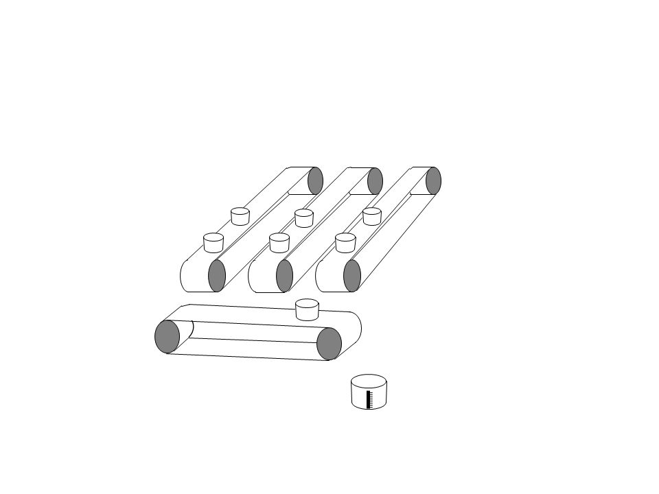
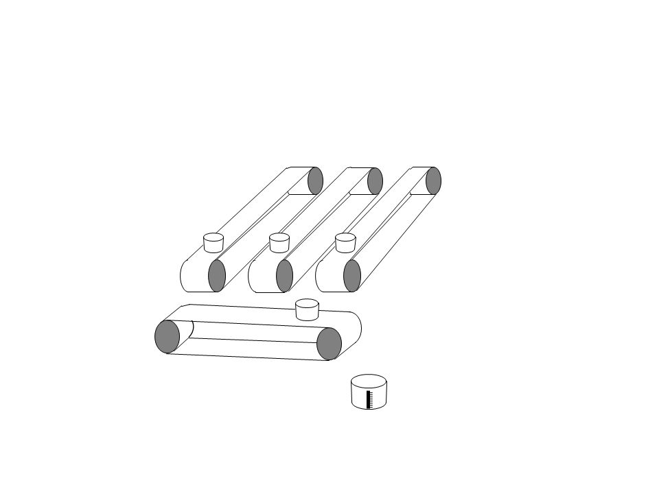
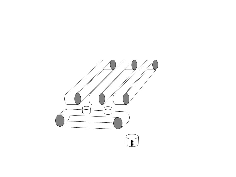
CCD Analogy A common analogy for the operation of a CCD is as follows:
An number of buckets (Pixels) are distributed across a field (Focal Plane of a telescope) in a square array. The buckets are placed on top of a series of parallel conveyor belts and collect rain fall (Photons) across the field. The conveyor belts are initially stationary, while the rain slowly fills the buckets (During the course of the exposure). Once the rain stops (The camera shutter closes) the conveyor belts start turning and transfer the buckets of rain , one by one , to a measuring cylinder (Electronic Amplifier) at the corner of the field (at the corner of the CCD) The animation in the following slides demonstrates how the conveyor belts work.
 are distributed across a field (Focal Plane of a telescope) in a square array. The buckets are placed on top of a series of parallel conveyor belts and collect rain fall. (Photons) across the field. The conveyor belts are initially stationary, while the rain slowly fills the. buckets (During the course of the exposure). Once the rain stops (The camera shutter closes) the. conveyor belts start turning and transfer the buckets of rain , one by one , to a measuring cylinder. (Electronic Amplifier) at the corner of the field (at the corner of the CCD) The animation in the following slides demonstrates how the conveyor belts work.")
6
CCD Analogy (SERIAL REGISTER) BUCKETS (PIXELS) HORIZONTAL
VERTICAL CONVEYOR BELTS (CCD COLUMNS) RAIN (PHOTONS) BUCKETS (PIXELS) MEASURING CYLINDER (OUTPUT AMPLIFIER) HORIZONTAL CONVEYOR BELT (SERIAL REGISTER)
![]()
7
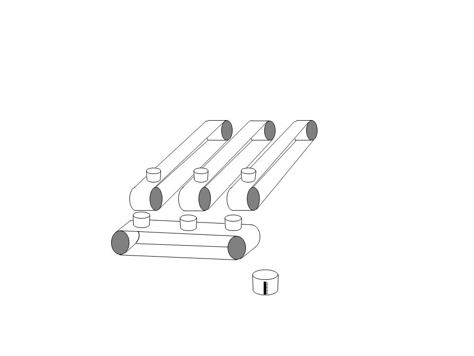
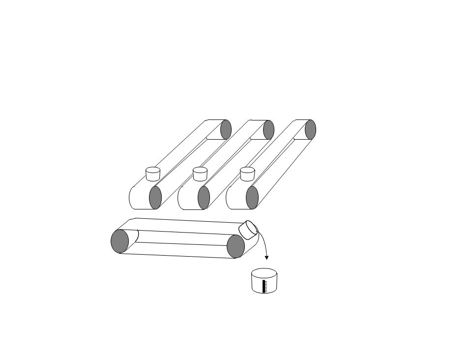
Exposure finished, buckets now contain samples of rain.

8
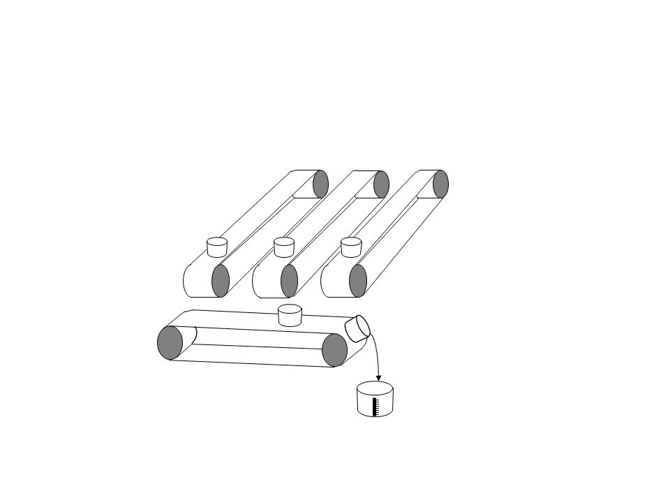
Conveyor belt starts turning and transfers buckets
Conveyor belt starts turning and transfers buckets. Rain collected on the vertical conveyor is tipped into buckets on the horizontal conveyor.

9
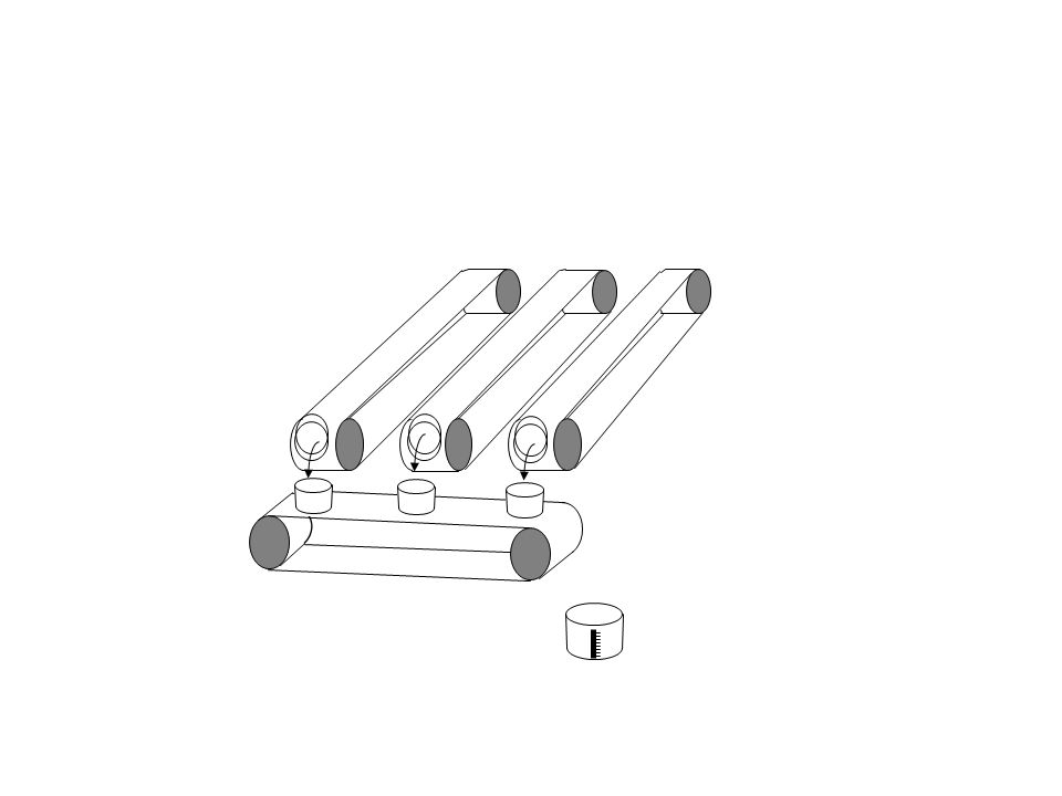
Vertical conveyor stops
Vertical conveyor stops. Horizontal conveyor starts up and tips each bucket in turn into the measuring cylinder .

10
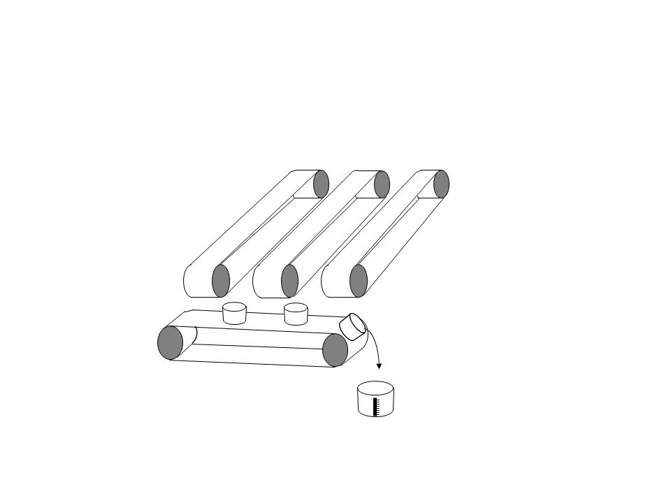
` After each bucket has been measured, the measuring cylinder
is emptied , ready for the next bucket load. `

17
A new set of empty buckets is set up on the horizontal conveyor and the process
is repeated.

34
Eventually all the buckets have been measured, the CCD has been read out.

35
Structure of a CCD 1. The image area of the CCD is positioned at the focal plane of the telescope. An image then builds up that consists of a pattern of electric charge. At the end of the exposure this pattern is then transferred, pixel at a time, by way of the serial register to the on-chip amplifier. Electrical connections are made to the outside world via a series of bond pads and thin gold wires positioned around the chip periphery. Image area Metal,ceramic or plastic package Connection pins Gold bond wires Bond pads Silicon chip On-chip amplifier Serial register

36
Structure of a CCD 2. CCDs are are manufactured on silicon wafers using the same photo-lithographic techniques used to manufacture computer chips. Scientific CCDs are very big ,only a few can be fitted onto a wafer. This is one reason that they are so costly. The photo below shows a silicon wafer with three large CCDs and assorted smaller devices. A CCD has been produced by Philips that fills an entire 6 inch wafer! It is the worlds largest integrated circuit. Don Groom LBNL

37
Structure of a CCD 3. Plan View Cross section
The diagram shows a small section (a few pixels) of the image area of a CCD. This pattern is repeated. Channel stops to define the columns of the image Plan View Transparent horizontal electrodes to define the pixels vertically. Also used to transfer the charge during readout One pixel Electrode Insulating oxide n-type silicon p-type silicon Cross section Every third electrode is connected together. Bus wires running down the edge of the chip make the connection. The channel stops are formed from high concentrations of Boron in the silicon.
 of the image area of a CCD. This pattern is repeated. Channel stops to define the columns of the image. Plan View. Transparent. horizontal electrodes. to define the pixels. vertically. Also. used to transfer the. charge during readout. One pixel. Electrode. Insulating oxide. n-type silicon. p-type silicon. Cross section. Every third electrode is connected together. Bus wires running down the edge of the chip make the. connection. The channel stops are formed from high concentrations of Boron in the silicon.")
39
Structure of a CCD 4. Image Area Cross section of serial register
Below the image area (the area containing the horizontal electrodes) is the ‘Serial register’ . This also consists of a group of small surface electrodes. There are three electrodes for every column of the image area Image Area On-chip amplifier at end of the serial register Serial Register Cross section of serial register Once again every third electrode is in the serial register connected together.
 is the ‘Serial register’ . This also. consists of a group of small surface electrodes. There are three electrodes for every column of the image area. Image Area. On-chip amplifier. at end of the serial. register. Serial Register. Cross section of. serial register. Once again every third electrode is in the serial register connected together.")
40
Structure of a CCD 5. Image Area Edge of Silicon Serial Register
160mm Photomicrograph of a corner of an EEV CCD. Image Area Serial Register Bus wires Edge of Silicon Read Out Amplifier The serial register is bent double to move the output amplifier away from the edge of the chip. This useful if the CCD is to be used as part of a mosaic.The arrows indicate how charge is transferred through the device.

41
Structure of a CCD 6. Output Drain (OD) 20mm Gate of Output Transistor
Photomicrograph of the on-chip amplifier of a Tektronix CCD and its circuit diagram. Output Drain (OD) 20mm Gate of Output Transistor Output Source (OS) SW R RD OD Output Node Reset Transistor Reset Drain (RD) Summing Well Output Node Output Transistor R Serial Register Electrodes OS Summing Well (SW) Substrate Last few electrodes in Serial Register
 20mm. Gate of Output Transistor. Output Source (OS) SW. R. RD. OD. Output Node. Reset. Transistor. Reset Drain (RD) Summing. Well. Output. Node. Output. Transistor. R. Serial Register Electrodes. OS. Summing Well (SW) Substrate. Last few electrodes in Serial Register.")
42
Electric Field in a CCD 1. The n-type layer contains an excess of electrons that diffuse into the p-layer. The p-layer contains an excess of holes that diffuse into the n-layer. This structure is identical to that of a diode junction. The diffusion creates a charge imbalance and induces an internal electric field. The electric potential reaches a maximum just inside the n-layer, and it is here that any photo-generated electrons will collect. All science CCDs have this junction structure, known as a ‘Buried Channel’. It has the advantage of keeping the photo-electrons confined away from the surface of the CCD where they could become trapped. It also reduces the amount of thermally generated noise (dark current). Electric potential Electric potential n p Potential along this line shown in graph above. Cross section through the thickness of the CCD
. Electric potential. Electric potential. n. p. Potential along this line shown. in graph above. Cross section through the thickness of the CCD.")
43
Electric Field in a CCD 2. During integration of the image, one of the electrodes in each pixel is held at a positive potential. This further increases the potential in the silicon below that electrode and it is here that the photoelectrons are accumulated. The neighboring electrodes, with their lower potentials, act as potential barriers that define the vertical boundaries of the pixel. The horizontal boundaries are defined by the channel stops. Electric potential Region of maximum potential n p
![]()
44
Charge Collection in a CCD.
Photons entering the CCD create electron-hole pairs. The electrons are then attracted towards the most positive potential in the device where they create ‘charge packets’. Each packet corresponds to one pixel boundary pixel incoming photons boundary pixel Electrode Structure n-type silicon Charge packet p-type silicon SiO2 Insulating layer

45
Conventional Clocking 1
Insulating layer Surface electrodes Charge packet (photo-electrons) N-type silicon P-type silicon Potential Energy Charge packets occupy potential minimums
 N-type silicon. P-type silicon. Potential Energy. Charge packets occupy potential minimums.")
46
Conventional Clocking 2
Potential Energy

47
Conventional Clocking 3
Potential Energy

48
Conventional Clocking 4
Potential Energy

49
Conventional Clocking 5
Potential Energy

50
Conventional Clocking 6
Potential Energy

51
Conventional Clocking 7
Potential Energy

52
Conventional Clocking 8
Potential Energy

53
Conventional Clocking 9
Potential Energy

54
Charge Transfer in a CCD 1.
In the following few slides, the implementation of the ‘conveyor belts’ as actual electronic structures is explained. The charge is moved along these conveyor belts by modulating the voltages on the electrodes positioned on the surface of the CCD. In the following illustrations, electrodes colour coded red are held at a positive potential, those coloured black are held at a negative potential. 1 2 3

55
Charge Transfer in a CCD 2.
+5V 0V -5V 2 +5V 0V -5V 1 +5V 0V -5V 3 1 2 3 Time-slice shown in diagram

56
Charge Transfer in a CCD 3.
+5V 0V -5V 2 +5V 0V -5V 1 +5V 0V -5V 3 1 2 3

57
Charge Transfer in a CCD 4.
+5V 0V -5V 2 +5V 0V -5V 1 +5V 0V -5V 3 1 2 3

58
Charge Transfer in a CCD 5.
+5V 0V -5V 2 +5V 0V -5V 1 +5V 0V -5V 3 1 2 3

59
Charge Transfer in a CCD 6.
+5V 0V -5V 2 +5V 0V -5V 1 +5V 0V -5V 3 1 2 3

60
Charge Transfer in a CCD 7.
+5V 0V -5V 2 Charge packet from subsequent pixel enters from left as first pixel exits to the right. +5V 0V -5V 1 +5V 0V -5V 3 1 2 3

61
Charge Transfer in a CCD 8.
+5V 0V -5V 2 +5V 0V -5V 1 +5V 0V -5V 3 1 2 3

62
On-Chip Amplifier 1. SW R Vout Vout
The on-chip amplifier measures each charge packet as it pops out the end of the serial register. RD and OD are held at constant voltages +5V 0V -5V SW SW R RD OD +10V 0V R Reset Transistor Vout Summing Well Output Node Output Transistor --end of serial register (The graphs above show the signal waveforms) OS The measurement process begins with a reset of the ‘reset node’. This removes the charge remaining from the previous pixel. The reset node is in fact a tiny capacitance (< 0.1pF) Vout
 OS. The measurement process begins with a reset. of the ‘reset node’. This removes the charge. remaining from the previous pixel. The reset. node is in fact a tiny capacitance (< 0.1pF) Vout.")
63
On-Chip Amplifier 2. SW R Vout Vout
The charge is then transferred onto the Summing Well. Vout is now at the ‘Reference level’ +5V 0V -5V SW SW R RD OD +10V 0V R Reset Transistor Vout Summing Well Output Node Output Transistor --end of serial register OS There is now a wait of up to a few tens of microseconds while external circuitry measures this ‘reference’ level. Vout

64
On-Chip Amplifier 3. SW R Vout Vout
The charge is then transferred onto the output node. Vout now steps down to the ‘Signal level’ +5V 0V -5V SW SW R RD OD +10V 0V R Reset Transistor Vout Summing Well Output Node Output Transistor --end of serial register OS This action is known as the ‘charge dump’ The voltage step in Vout is as much as several mV for each electron contained in the charge packet. Vout

65
On-Chip Amplifier 4. Vout is now sampled by external circuitry for up to a few tens of microseconds. +5V 0V -5V SW SW R RD OD +10V 0V R Reset Transistor Vout Summing Well Output Node Output Transistor --end of serial register OS The sample level - reference level will be proportional to the size of the input charge packet. Vout

66
Quantum Efficiency Readout Electronics Device Defects Data Processing
CCD: Advanced Topics 1 Quantum Efficiency Readout Electronics Device Defects Data Processing

67
Thick Front-side Illuminated CCD
Incoming photons p-type silicon n-type silicon Silicon dioxide insulating layer 625mm Polysilicon electrodes These are cheap to produce using conventional wafer fabrication techniques. They are used in consumer imaging applications. Even though not all the photons are detected, these devices are still more sensitive than photographic film. They have a low Quantum Efficiency due to the reflection and absorption of light in the surface electrodes. Very poor blue response. The electrode structure prevents the use of an Anti-reflective coating that would otherwise boost performance. The amateur astronomer on a limited budget might consider using thick CCDs. For professional observatories, the economies of running a large facility demand that the detectors be as sensitive as possible; thick front-side illuminated chips are seldom if ever used.

68
[ ] nt-ni ni = nt+ni nt Anti-Reflection Coatings 1
Silicon has a very high Refractive Index (denoted by n). This means that photons are strongly reflected from its surface. [ ] nt-ni nt+ni 2 ni Fraction of photons reflected at the interface between two mediums of differing refractive indices = nt n of air or vacuum is 1.0, glass is 1.46, water is 1.33, Silicon is 3.6. Using the above equation we can show that window glass in air reflects 3.5% and silicon in air reflects 32%. Unless we take steps to eliminate this reflected portion, then a silicon CCD will at best only detect 2 out of every 3 photons. The solution is to deposit a thin layer of a transparent dielectric material on the surface of the CCD. The refractive index of this material should be between that of silicon and air, and it should have an optical thickness = 1/4 wavelength of light. The question now is what wavelength should we choose, since we are interested in a wide range of colours. Typically 550nm is chosen, which is close to the middle of the optical spectrum.
![[ ] nt-ni ni = nt+ni nt Anti-Reflection Coatings 1](http://slideplayer.com/slide/4936296/16/images/68/%5B+%5D+nt-ni+ni+%3D+nt%2Bni+nt+Anti-Reflection+Coatings+1.jpg "Silicon has a very high Refractive Index (denoted by n). This means that photons are strongly reflected. from its surface. [ ] nt-ni. nt+ni. 2. ni. Fraction of photons reflected at the. interface between two mediums of. differing refractive indices. = nt. n of air or vacuum is 1.0, glass is 1.46, water is 1.33, Silicon is 3.6. Using the above equation we can. show that window glass in air reflects 3.5% and silicon in air reflects 32%. Unless we take steps to. eliminate this reflected portion, then a silicon CCD will at best only detect 2 out of every 3 photons. The solution is to deposit a thin layer of a transparent dielectric material on the surface of the CCD. The. refractive index of this material should be between that of silicon and air, and it should have an. optical thickness = 1/4 wavelength of light. The question now is what wavelength should we choose, since. we are interested in a wide range of colours. Typically 550nm is chosen, which is close to the middle of the. optical spectrum.")
69
[ ] ni ns nt nt x ni-ns nt x ni+ns ns nt Anti-Reflection Coatings 2 =
With an Anti-reflective coating we now have three mediums to consider : ni Air ns AR Coating nt Silicon [ ] nt x ni-ns 2 nt x ni+ns The reflected portion is now reduced to : In the case where the reflectivity actually falls to zero! For silicon we require a material with n = 1.9, fortunately such a material exists, it is Hafnium Dioxide. It is regularly used to coat astronomical CCDs. ns nt 2 =
![[ ] ni ns nt nt x ni-ns nt x ni+ns ns nt Anti-Reflection Coatings 2 =](http://slideplayer.com/slide/4936296/16/images/69/%5B+%5D+ni+ns+nt+nt+x+ni-ns+nt+x+ni%2Bns+ns+nt+Anti-Reflection+Coatings+2+%3D.jpg "With an Anti-reflective coating we now have three mediums to consider : ni. Air. ns. AR Coating. nt. Silicon. [ ] nt x ni-ns. 2. nt x ni+ns. The reflected portion is now reduced to : In the case where the reflectivity actually falls to zero! For silicon we require a material. with n = 1.9, fortunately such a material exists, it is Hafnium Dioxide. It is regularly used to coat. astronomical CCDs. ns. nt. 2. =")
70
Anti-Reflection Coatings 3
The graph below shows the reflectivity of an EEV CCD. These thinned CCDs were designed for a maximum blue response and it has an anti-reflective coating optimised to work at 400nm. At this wavelength the reflectivity falls to approximately 1%.

71
Thinned Back-side Illuminated CCD
Anti-reflective (AR) coating Incoming photons p-type silicon n-type silicon Silicon dioxide insulating layer 15mm Polysilicon electrodes The silicon is chemically etched and polished down to a thickness of about 15microns. Light enters from the rear and so the electrodes do not obstruct the photons. The QE can approach 100% . These are very expensive to produce since the thinning is a non-standard process that reduces the chip yield. These thinned CCDs become transparent to near infra-red light and the red response is poor. Response can be boosted by the application of an anti-reflective coating on the thinned rear-side. These coatings do not work so well for thick CCDs due to the surface bumps created by the surface electrodes. Almost all Astronomical CCDs are Thinned and Backside Illuminated.
 coating. Incoming photons. p-type silicon. n-type silicon. Silicon dioxide insulating layer. 15mm. Polysilicon electrodes. The silicon is chemically etched and polished down to a thickness of about 15microns. Light enters. from the rear and so the electrodes do not obstruct the photons. The QE can approach 100% . These are very expensive to produce since the thinning is a non-standard process that reduces the. chip yield. These thinned CCDs become transparent to near infra-red light and the red response is. poor. Response can be boosted by the application of an anti-reflective coating on the thinned. rear-side. These coatings do not work so well for thick CCDs due to the surface bumps created. by the surface electrodes. Almost all Astronomical CCDs are Thinned and Backside Illuminated.")
72
Quantum Efficiency Comparison
The graph below compares the quantum of efficiency of a thick frontside illuminated CCD and a thin backside illuminated CCD.

73
‘Internal’ Quantum Efficiency
If we take into account the reflectivity losses at the surface of a CCD we can produce a graph showing the ‘internal QE’ : the fraction of the photons that enter the CCDs bulk that actually produce a detected photo-electron. This fraction is remarkably high for a thinned CCD. For the EEV CCD, shown below, it is greater than 85% across the full visible spectrum. Todays CCDs are very close to being ideal visible light detectors!

74
Appearance of CCDs The fine surface electrode structure of a thick CCD is clearly visible as a multi-coloured interference pattern. Thinned Backside Illuminated CCDs have a much planer surface appearance. The other notable distinction is the two-fold (at least) price difference. Kodak Kaf1401 Thick CCD MIT/LL CC1D20 Thinned CCD
 price difference. Kodak Kaf1401 Thick CCD MIT/LL CC1D20 Thinned CCD.")
75
UV-Sensitive Silicon Detectors
UV (<400 nm) is challenging Shallow penetration depth of radiation (<10 nm at = nm) Requires extremely thin, doped surface layer
 is challenging. Shallow penetration depth of radiation (<10 nm at = nm) Requires extremely thin, doped surface layer.")
76
Ultra-high-vacuum MBE system
Back-Illumination Process for Enhanced UV Performance Rim-thinned silicon wafer Ultra-high-vacuum MBE system

77
Quantum-Efficiency Results

78
Quantum Efficiency of AR-coated MBE Devices
HfO2 (optimized for ~330 nm) HfO2/SiO2 (broadband, low fringing) MBE processed Device thickness=45µm T=20°C
 HfO2/SiO2 (broadband, low fringing) MBE processed. Device thickness=45µm. T=20°C.")
79
Temperature Dependence of Quantum Efficiency Near Band Edge

80
Si Bandstructure: Indirect

81
Ga-As Bandstructure: Direct

82
Ultra-high-vacuum MBE system
Back-Illumination Process for Enhanced UV Performance Rim-thinned silicon wafer Ultra-high-vacuum MBE system

83
Deep Depletion CCDs 1. The electric field structure in a CCD defines to a large degree its Quantum Efficiency (QE). Consider first a thick frontside illuminated CCD, which has a poor QE. Electric potential Potential along this line shown in graph above. Cross section through a thick frontside illuminated CCD In this region the electric potential gradient is fairly low i.e. the electric field is low. Any photo-electrons created in the region of low electric field stand a much higher chance of recombination and loss. There is only a weak external field to sweep apart the photo-electron and the hole it leaves behind.

84
Deep Depletion CCDs 2. In a thinned CCD , the field free region is simply etched away. Cross section through a thinned CCD Electric potential Electric potential There is now a high electric field throughout the full depth of the CCD. Problem : Thinned CCDs may have good blue response but they become transparent at longer wavelengths; the red response suffers. This volume is etched away during manufacture Red photons can now pass right through the CCD. Photo-electrons created anywhere throughout the depth of the device will now be detected. Thinning is normally essential with backside illuminated CCDs if good blue response is required. Most blue photo-electrons are created within a few nanometers of the surface and if this region is field free, there will be no blue response.

85
Deep Depletion CCDs 3. Ideally we require all the benefits of a thinned CCD plus an improved red response. The solution is to use a CCD with an intermediate thickness of about 40mm constructed from Hi-Resistivity silicon. The increased thickness makes the device opaque to red photons. The use of Hi-Resistivity silicon means that there are no field free regions despite the greater thickness. Cross section through a Deep Depletion CCD Electric potential Electric potential Problem : Hi resistivity silicon contains much lower impurity levels than normal. Very few wafer fabrication factories commonly use this material and deep depletion CCDs have to be designed and made to order. Red photons are now absorbed in the thicker bulk of the device. There is now a high electric field throughout the full depth of the CCD. CCDs manufactured in this way are known as Deep depletion CCDs. The name implies that the region of high electric field, also known as the ‘depletion zone’ extends deeply into the device.

86
Deep Depletion CCDs 4. The graph below shows the improved QE response available from a deep depletion CCD. The black curve represents a normal thinned backside illuminated CCD. The Red curve is actual data from a deep depletion chip manufactured by MIT Lincoln Labs. This latter chip is still under development.The blue curve suggests what QE improvements could eventually be realised in the blue end of the spectrum once the process has been perfected.

87
Deep Depletion CCDs 5. Another problem commonly encountered with thinned CCDs is ‘fringing’. The is greatly reduced in deep depletion CCDs. Fringing is caused by multiple reflections inside the CCD. At longer wavelengths, where thinned chips start to become transparent, light can penetrate through and be reflected from the rear surface. It then interferes with light entering for the first time. This can give rise to constructive and destructive interference and a series of fringes where there are minor differences in the chip thickness. The image below shows some fringes from an EEV42-80 thinned CCD For spectroscopic applications, fringing can render some thinned CCDs unusable, even those that have quite respectable QEs in the red. Thicker deep depletion CCDs , which have a much lower degree of internal reflection and much lower fringing are preferred by astronomers for spectroscopy.

88
LBNL 2k x 2k Quantum Efficiency
2 layer anti-reflection coating: ~ 600A ITO, ~1000A SiO2

89
Fully-depleted pin diode radiation detector
Photons: Near IR – Visible: 1 electron hole pair/photon UV/x ray/g ray: E(eV)/3.6 electron hole pairs/photon To Amplifier VSUB ~ 80 electron hole pairs/mm for minimum ionizing particles (High Energy Physics) Slope r/esi = qND/esi Over depleted
/3.6 electron hole pairs/photon. To Amplifier. VSUB. ~ 80 electron hole. pairs/mm for minimum. ionizing particles. (High Energy Physics) Slope r/esi = qND/esi. Over depleted.")
90
LBNL 2k x 4k (100mm wafer) Measurements at Lick Observatory
 Measurements at Lick Observatory")
91
Fully-depleted, back-illuminated 1024 x 512 (15mm)2 CCD fabricated at Dalsa Semi
30 minute dark (3 e-/pixel-hr at –150C) 500nm flat field 400nm flat field All at 80V Vsub (overdepleted)
 500nm flat field. 400nm flat field. All at 80V Vsub (overdepleted)")
92
Visible vs Near-IR imaging

93
LBNL 2k x 2k results Image: 200 x m LBNL CCD in Lick Nickel 1m. Spectrum: 800 x m LBNL CCD in NOAO KPNO spectrograph. Instrument at NOAO KPNO 2nd semester 2001 (

94
Correlated Double Sampler (CDS) 1.
The video waveform output by a CCD is at a fairly low level : every photo-electron in a pixel charge packet will produce a few micro-volts of signal. Additionally, the waveform is complex and precise timing is required to make sure that the correct parts are amplified and measured. The CCD video waveform , as introduced in Activity 1, is shown below for the period of one pixel measurement Vout t Reset feedthrough Reference level Charge dump Signal level The video processor must measure , without introducing any additional noise, the Reference level and the Signal level. The first is then subtracted from the second to yield the output signal voltage proportional to the number of photo-electrons in the pixel under measurement. The best way to perform this processing is to use a ‘Correlated Double Sampler’ or CDS.

95
. Correlated Double Sampler (CDS) 2. ADC -1 Reset switch
The CDS design is shown schematically below. The CDS processes the video waveform and outputs a digital number proportional to the size of the charge packet contained in the pixel being read. There should only be a short cable length between CCD and CDS to minimise noise.The CDS minimises the read noise of the CCD by eliminating ‘reset noise’. The CDS contains a high speed analogue processor containing computer controlled switches. Its output feeds into an Analogue to Digital Converter (ADC). OD OS RD R Reset switch CCD On-chip Amplifier Integrator Pre-Amplifier Inverting Amplifier . -1 Computer Bus ADC Input Switch Polarity Switch
. OD. OS. RD. R. Reset switch. CCD On-chip Amplifier. Integrator. Pre-Amplifier. Inverting Amplifier Computer Bus. ADC. Input Switch. Polarity Switch.")
96
Correlated Double Sampler (CDS) 3.
The CDS starts work once the pixel charge packet is in the CCD summing well and the CCD reset pulse has just finished. At point t0 the CCD wave-form is still affected by the reset pulse and so the CDS remains disconnected from the CCD to prevent this disturbing the video processor. t0 t0 Output wave-form of CCD Output voltage of CDS -1

97
Correlated Double Sampler (CDS) 4.
Between t1 and t2 the CDS is connected and the ‘Reference ‘ part of the waveform is sampled. Simultaneously the integrator reset switch is opened and the output starts to ramp down linearly. t1 t2 t1 t2 Reference window -1

98
Correlated Double Sampler (CDS) 5.
Between t2 and t3 the ‘charge dump’ occurs in the CCD. The CCD output steps negatively by an amount proportional to the charge contained in the pixel. During this time the CDS is disconnected. t2 t3 t1 t2 t3 -1

99
Correlated Double Sampler (CDS) 6.
Between t3 and t4 the CDS is reconnected and the ‘signal’ part of the wave-form is sampled. The input to the integrator is also ‘polarity switched’ so that the CDS output starts to ramp-up linearly. The width of the signal and sample windows must be the same. For Scientific CCDs this can be anything between 1 and 20 microseconds. Longer widths generally give lower noise but of course increase the read-out time. t3 t4 t1 t2 t3 t4 Signal window -1

100
Correlated Double Sampler (CDS) 7.
The CDS is then once again disconnected and its output digitised by the ADC. This number , typically a 16 bit number (with a value between 0 and 65535) is then stored in the computer memory. The CDS then starts the whole process again on the next pixel. The integrator output is first zeroed by closing the reset switch. To process each pixel can take between a fraction of a microsecond for a TV rate CCD and several tens of microseconds for a low noise scientific CCD. The type of CDS is called a ‘dual slope integrator’. A simpler type of CDS known as a ‘clamp and sample’ only samples the waveform once for each pixel. It works well at higher pixel rates but is noisier than the dual slope integrator at lower pixel rates. t1 t2 t3 t4 Voltage to be digitised -1 ADC
 is then stored in the computer memory. The CDS. then starts the whole process again on the next pixel. The integrator output is first zeroed by closing. the reset switch. To process each pixel can take between a fraction of a microsecond for a. TV rate CCD and several tens of microseconds for a low noise scientific CCD. The type of CDS is called a ‘dual slope integrator’. A simpler type of CDS known as a ‘clamp and sample’ only samples the waveform once for each pixel. It works well at higher pixel rates but is noisier. than the dual slope integrator at lower pixel rates. t1. t2. t3. t4. Voltage to be. digitised. -1. ADC.")
101
Pixel Size and Binning 6. The first row is transferred into the serial register
![]()
102
Pixel Size and Binning 5. Stage 1 :Vertical Binning
This is done by summing the charge in consecutive rows .The summing is done in the serial register. In the case of 2 x 2 binning, two image rows will be clocked consecutively into the serial register prior to the serial register being read out. We now go back to the conveyor belt analogy of a CCD. In the following animation we see the bottom two image rows being binned. Charge packets
![]()
103
Pixel Size and Binning 7. The serial register is kept stationary ready for the next row to be transferred.
![]()
104
Pixel Size and Binning 8. The second row is now transferred into the serial register.
![]()
105
Pixel Size and Binning 9. Each pixel in the serial register now contains the charge from two pixels in the image area. It is thus important that the serial register pixels have a higher charge capacity. This is achieved by giving them a larger physical size.
![]()
106
Pixel Size and Binning 10. SW 1 2 3 Stage 2 :Horizontal Binning
This is done by combining charge from consecutive pixels in the serial register on a special electrode positioned between serial register and the readout amplifier called the Summing Well (SW). The animation below shows the last two pixels in the serial register being binned : SW 1 2 Output Node 3
![]()
107
Pixel Size and Binning 11. SW 1 2 3
Charge is clocked horizontally with the SW held at a positive potential. SW 1 2 Output Node 3
![]()
108
Pixel Size and Binning 12. SW 1 2 Output Node 3
![]()
109
Pixel Size and Binning 13. SW 1 2 Output Node 3
![]()
110
Pixel Size and Binning 14. SW 1 2 3
The charge from the first pixel is now stored on the summing well. SW 1 2 Output Node 3
![]()
111
Pixel Size and Binning 15. SW 1 2 3
The serial register continues clocking. SW 1 2 Output Node 3
![]()
112
Pixel Size and Binning 16. SW 1 2 Output Node 3
![]()
113
Pixel Size and Binning 17. SW 1 2 3
The SW potential is set slightly higher than the serial register electrodes. SW 1 2 Output Node 3
![]()
114
Pixel Size and Binning 18. SW 1 2 Output Node 3
![]()
115
Pixel Size and Binning 19. SW 1 2 3
The charge from the second pixel is now transferred onto the SW. The binning is now complete and the combined charge packet can now be dumped onto the output node (by pulsing the voltage on SW low for a microsecond) for measurement. Horizontal binning can also be done directly onto the output node if a SW is not present but this can increase the read noise. SW 1 2 Output Node 3
![]()
116
Pixel Size and Binning 20. SW 1 2 3
Finally the charge is dumped onto the output node for measurement SW 1 2 Output Node 3
![]()
117
Noise Sources in a CCD Image 1.
The main noise sources found in a CCD are : READ NOISE. Caused by electronic noise in the CCD output transistor and possibly also in the external circuitry. Read noise places a fundamental limit on the performance of a CCD. It can be reduced at the expense of increased read out time. Scientific CCDs have a readout noise of 2-3 electrons RMS. 2. DARK CURRENT. Caused by thermally generated electrons in the CCD. Eliminated by cooling the CCD. 3. PHOTON NOISE. Also called ‘Shot Noise’. It is due to the fact that the CCD detects photons. Photons arrive in an unpredictable fashion described by Poissonian statistics. This unpredictability causes noise. 4. PIXEL RESPONSE NON-UNIFORMITY. Defects in the silicon and small manufacturing defects can cause some pixels to have a higher sensitivity than their neighbours. This noise source can be removed by ‘Flat Fielding’; an image processing technique.

118
Noise Sources in a CCD Image 2.
Before these noise sources are explained further some new terms need to be introduced. FLAT FIELDING This involves exposing the CCD to a very uniform light source that produces a featureless and even exposure across the full area of the chip. A flat field image can be obtained by exposing on a twilight sky or on an illuminated white surface held close to the telescope aperture (for example the inside of the dome). Flat field exposures are essential for the reduction of astronomical data. BIAS REGIONS A bias region is an area of a CCD that is not sensitive to light. The value of pixels in a bias region is determined by the signal processing electronics. It constitutes the zero-signal level of the CCD. The bias region pixels are subject only to readout noise. Bias regions can be produced by ‘over-scanning’ a CCD, i.e. reading out more pixels than are actually present. Designing a CCD with a serial register longer than the width of the image area will also create vertical bias strips at the left and right sides of the image. These strips are known as the ‘x-underscan’ and ‘x-overscan’ regions A flat field image containing bias regions can yield valuable information not only on the various noise sources present in the CCD but also about the gain of the signal processing electronics i.e. the number of photoelectrons represented by each digital unit (ADU) output by the camera’s Analogue to Digital Converter.
. Flat field exposures are essential for the reduction of astronomical data. BIAS REGIONS. A bias region is an area of a CCD that is not sensitive to light. The value of pixels in a bias region. is determined by the signal processing electronics. It constitutes the zero-signal level of the CCD. The bias region pixels are subject only to readout noise. Bias regions can be produced by. ‘over-scanning’ a CCD, i.e. reading out more pixels than are actually present. Designing a CCD with. a serial register longer than the width of the image area will also create vertical bias strips at the left. and right sides of the image. These strips are known as the ‘x-underscan’ and ‘x-overscan’ regions. A flat field image containing bias regions can yield valuable information not only on the various. noise sources present in the CCD but also about the gain of the signal processing electronics. i.e. the number of photoelectrons represented by each digital unit (ADU) output by the camera’s. Analogue to Digital Converter.")
119
Noise Sources in a CCD Image 3.
Flat field images obtained from two CCD geometries are represented below. The arrows represent the position of the readout amplifier and the thick black line at the bottom of each image represents the serial register. Y-overscan CCD With Serial Register equal in length to the image area width. Here, the CCD is over-scanned in X and Y Image Area X-overscan Y-overscan Here, the CCD is over-scanned in Y to produce the Y-overscan bias area. The X-underscan and X-overscan are created by extensions to the serial register on either side of the image area. When charge is transferred from the image area into the serial register, these extensions do not receive any photo-charge. CCD With Serial Register greater in length than the image area width. X-underscan X-overscan Image Area

120
Noise Sources in a CCD Image 4.
These four noise sources are now explained in more detail: READ NOISE. This is mainly caused by thermally induced motions of electrons in the output amplifier. These cause small noise voltages to appear on the output. This noise source, known as Johnson Noise, can be reduced by cooling the output amplifier or by decreasing its electronic bandwidth. Decreasing the bandwidth means that we must take longer to measure the charge in each pixel, so there is always a trade-off between low noise performance and speed of readout. Mains pickup and interference from circuitry in the observatory can also contribute to Read Noise but can be eliminated by careful design. Johnson noise is more fundamental and is always present to some degree. The graph below shows the trade-off between noise and readout speed for an EEV4280 CCD.

121
Noise Sources in a CCD Image 5.
DARK CURRENT. Electrons can be generated in a pixel either by thermal motion of the silicon atoms or by the absorption of photons. Electrons produced by these two effects are indistinguishable. Dark current is analogous to the fogging that can occur with photographic emulsion if the camera leaks light. Dark current can be reduced or eliminated entirely by cooling the CCD. Science cameras are typically cooled with liquid nitrogen to the point where the dark current falls to below 1 electron per pixel per hour where it is essentially un-measurable. Amateur cameras cooled thermoelectrically may still have substantial dark current. The graph below shows how the dark current of a TEK1024 CCD can be reduced by cooling.

122
Noise Sources in a CCD Image 6.
PHOTON NOISE. This can be understood more easily if we go back to the analogy of rain drops falling onto an array of buckets; the buckets being pixels and the rain drops photons. Both rain drops and photons arrive discretely, independently and randomly and are described by Poissonian statistics. If the buckets are very small and the rain fall is very sparse, some buckets may collect one or two drops, others may collect none at all. If we let the rain fall long enough all the buckets will measure the same value , but for short measurement times the spread in measured values is large. This latter scenario is essentially that of CCD astronomy where small pixels are collecting very low fluxes of photons. Poissonian statistics tells us that the Root Mean square uncertainty (RMS noise) in the number of photons per second detected by a pixel is equal to the square root of the mean photon flux (the average number of photons detected per second). For example, if a star is imaged onto a pixel and it produces on average 10 photo-electrons per second and we observe the star for 1 second, then the uncertainty of our measurement of its brightness will be the square root of 10 i.e. 3.2 electrons. This value is the ‘Photon Noise’. Increasing exposure time to 100 seconds will increase the photon noise to 10 electrons (the square root of 100) but at the same time will increase the ‘Signal to Noise ratio’ (SNR). In the absence of other noise sources the SNR will increase as the square root of the exposure time. Astronomy is all about maximising the SNR. { Dark current, described earlier, is also governed by Poissonian statistics. If the mean dark current contribution to an image is 900 electrons per pixel, the noise introduced into the measurement of any pixels photo-charge would be 30 electrons }
 in the number of. photons per second detected by a pixel is equal to the square root of the mean photon flux (the. average number of photons detected per second). For example, if a star is imaged onto a pixel and it produces on average 10 photo-electrons per. second and we observe the star for 1 second, then the uncertainty of our measurement of its brightness. will be the square root of 10 i.e. 3.2 electrons. This value is the ‘Photon Noise’. Increasing exposure time to 100 seconds will increase the photon noise to 10 electrons (the square root. of 100) but at the same time will increase the ‘Signal to Noise ratio’ (SNR). In the absence of other. noise sources the SNR will increase as the square root of the exposure time. Astronomy is all about. maximising the SNR. { Dark current, described earlier, is also governed by Poissonian statistics. If the mean dark current. contribution to an image is 900 electrons per pixel, the noise introduced into the measurement. of any pixels photo-charge would be 30 electrons }")
123
Noise Sources in a CCD Image 7.
PIXEL RESPONSE NON-UNIFORMITY (PRNU). If we take a very deep (at least 50,000 electrons of photo-generated charge per pixel) flat field exposure , the contribution of photon noise and read noise become very small. If we then plot the pixel values along a row of the image we see a variation in the signal caused by the slight variations in sensitivity between the pixels. The graph below shows the PRNU of an EEV4280 CCD illuminated by blue light. The variations are as much as +/-2%. Fortunately these variations are constant and are easily removed by dividing a science image, pixel by pixel, by a flat field image.
. If we take a very deep (at least 50,000 electrons of photo-generated charge per pixel) flat field exposure , the contribution of photon noise and read noise become very small. If we then plot the pixel values. along a row of the image we see a variation in the signal caused by the slight variations in sensitivity. between the pixels. The graph below shows the PRNU of an EEV4280 CCD illuminated by blue light. The variations are as much as +/-2%. Fortunately these variations are constant and are easily removed. by dividing a science image, pixel by pixel, by a flat field image.")
124
Noise Sources in a CCD Image 8.
HOW THE VARIOUS NOISE SOURCES COMBINE Assuming that the PRNU has been removed by flat fielding, the three remaining noise sources combine in the following equation: In professional systems the dark current tends to zero and this term of the equation can be ignored. The equation then shows that read noise is only significant in low signal level applications such as Spectroscopy. At higher signal levels, such as those found in direct imaging, the photon noise becomes increasingly dominant and the read noise becomes insignificant. For example , a CCD with read noise of 5 electrons RMS will become photon noise dominated once the signal level exceeds 25 electrons per pixel. If the exposure is continued to a level of 100 electrons per pixel, the read noise contributes only 11% of the total noise. NOISEtotal = (READ NOISE)2 + (PHOTON NOISE)2 +(DARK CURRENT)2
2 + (PHOTON NOISE)2 +(DARK CURRENT)2.")
125
Noise Calibration Definitions: N_ad - Noise in A/D converter units
N_e - Noise in electrons S_ad - Signal in A/D converter units S_e - Signal in electrons g Gain factor (electrons/adu) S_e = g × S_ad N_e = g × N_ad g²×(N_ad)² = (g × N_ad)² = (N_e)² = S_e = g × S_ad g = S_ad / (N_ad)²
 S_e = g × S_ad N_e = g × N_ad. g²×(N_ad)² = (g × N_ad)² = (N_e)² = S_e = g × S_ad. g = S_ad / (N_ad)².")
126
Principle of Aperture Photometry
Star Aperture Sky Annulus Signal in aperture: Star + aperture_area x sky_average Signal in Annulus: annulus_area x sky_average Signal of Star: aperture_signal – aperture_area x sky_average

127
V-band sky brightness variations

128
Blooming in a CCD 1. The charge capacity of a CCD pixel is limited, when a pixel is full the charge starts to leak into adjacent pixels. This process is known as ‘Blooming’. Spillage Spillage boundary pixel boundary pixel Overflowing charge packet Photons Photons
![]()
129
Blooming in a CCD 2. The diagram shows one column of a CCD with an over-exposed stellar image focused on one pixel. The channel stops shown in yellow prevent the charge spreading sideways. The charge confinement provided by the electrodes is less so the charge spreads vertically up and down a column. The capacity of a CCD pixel is known as the ‘Full Well’. It is dependent on the physical area of the pixel. For Tektronix CCDs, with pixels measuring 24mm x 24mm it can be as much as 300,000 electrons. Bloomed images will be seen particularly on nights of good seeing where stellar images are more compact . In reality, blooming is not a big problem for professional astronomy. For those interested in pictorial work, however, it can be a nuisance. bloomed Flow of charge
![]()
130
Blooming in a CCD 3. The image below shows an extended source with bright embedded stars. Due to the long exposure required to bring out the nebulosity, the stellar images are highly overexposed and create bloomed images. M42 Bloomed star images (The image is from a CCD mosaic and the black strip down the center is the space between adjacent detectors)
")
131
Image Defects in a CCD 1. Unless one pays a huge amount it is generally difficult to obtain a CCD free of image defects. The first kind of defect is a ‘dark column’. Their locations are identified from flat field exposures. Dark columns are caused by ‘traps’ that block the vertical transfer of charge during image readout. The CCD shown at left has at least 7 dark columns, some grouped together in adjacent clusters. Traps can be caused by crystal boundaries in the silicon of the CCD or by manufacturing defects. Although they spoil the chip cosmetically, dark columns are not a big problem for astronomers. This chip has 2048 image columns so 7 bad columns represents a tiny loss of data. Flat field exposure of an EEV42-80 CCD

132
Image Defects in a CCD 2. There are three other common image defect types : Cosmic rays, Bright columns and Hot Spots. Their locations are shown in the image below which is a lengthy exposure taken in the dark (a ‘Dark Frame’) Bright columns are also caused by traps . Electrons contained in such traps can leak out during readout causing a vertical streak. Hot Spots are pixels with higher than normal dark current. Their brightness increases linearly with exposure times Cosmic rays are unavoidable. Charged particles from space or from radioactive traces in the material of the camera can cause ionisation in the silicon. The electrons produced are indistinguishable from photo-generated electrons. Approximately 2 cosmic rays per cm2 per minute will be seen. A typical event will be spread over a few adjacent pixels and contain several thousand electrons. Somewhat rarer are light-emitting defects which are hot spots that act as tiny LEDS and cause a halo of light on the chip. Bright Column Cluster of Hot Spots Cosmic rays 900s dark exposure of an EEV42-80 CCD
 Bright columns are also caused by traps . Electrons contained. in such traps can leak out during readout causing a vertical streak. Hot Spots are pixels with higher than normal dark current. Their. brightness increases linearly with exposure times. Cosmic rays are unavoidable. Charged particles from space or. from radioactive traces in the material of the camera can. cause ionisation in the silicon. The electrons produced are. indistinguishable from photo-generated electrons. Approximately 2 cosmic rays per cm2 per minute will be seen. A typical event will be spread over a few adjacent pixels and. contain several thousand electrons. Somewhat rarer are light-emitting defects which are hot spots. that act as tiny LEDS and cause a halo of light on the chip. Bright. Column. Cluster of. Hot Spots. Cosmic rays. 900s dark exposure of an EEV42-80 CCD.")
133
Image Defects in a CCD 3. Some defects can arise from the processing electronics. This negative image has a bright line in the first image row. M51 Dark column Hot spots and bright columns Bright first image row caused by incorrect operation of signal processing electronics.

134
Biases, Flat Fields and Dark Frames 1.
These are three types of calibration exposures that must be taken with a scientific CCD camera, generally before and after each observing session. They are stored alongside the science images and combined with them during image processing. These calibration exposures allow us to compensate for certain imperfections in the CCD. As much care needs to be exercised in obtaining these images as for the actual scientific exposures. Applying low quality flat fields and bias frames to scientific data can degrade rather than improve its quality. Bias Frames A bias frame is an exposure of zero duration taken with the camera shutter closed. It represents the zero point or base-line signal from the CCD. Rather than being completely flat and featureless the bias frame may contain some structure. Any bright image defects in the CCD will of course show up, there may be also slight gradients in the image caused by limitations in the signal processing electronics of the camera. It is normal to take about 5 bias frames before a night’s observing. These are then combined using an image processing algorithm that averages the images, pixel by pixel, rejecting any pixel values that are appreciably different from the other 4. This can happen if a pixel in one bias frame is affected by a cosmic ray event. It is unlikely that the same pixel in the other 4 frames would be similarly affected so the resultant ‘master bias’, should be uncontaminated by cosmic rays. Taking a number of biases and then averaging them also reduces the amount of noise in the bias images. Averaging 5 frames will reduce the amount of read noise (electronic noise from the CCD amplifier) in the image by the square-root of 5.
 in the image by the square-root of 5.")
135
Biases, Flat Fields and Dark Frames 3.
A dark frame and a flat field from the same EEV42-80 CCD are shown below. The dark frame shows a number of bright defects on the chip. The flat field shows a criss-cross patterning on the chip created during manufacture and a slight loss of sensitivity in two corners of the image. Some dust spots are also visible. Dark Frame Flat Field

136
Biases, Flat Fields and Dark Frames 4.
If there is significant dark current present, the various calibration and science frames are combined by the following series of subtractions and divisions : Science Frame Dark Frame Science -Dark Output Image Flat Field Image Science -Dark Flat-Bias Flat -Bias Bias Image

137
Dark Frames and Flat Fields 5.
In the absence of dark current, the process is slightly simpler : Science Frame Science -Bias Bias Image Output Image Science -Bias Flat-Bias Flat -Bias Flat Field Image

Similar presentations


>")


 AS3100 Lab. Astronomi Dasar I Prodi Astronomi 2007/2008 B. Dermawan.>")


 BUCKETS (PIXELS) VERTICAL CONVEYOR BELTS (CCD COLUMNS) HORIZONTAL CONVEYOR BELT ( SERIAL REGISTER ) MEASURING CYLINDER (OUTPUT AMPLIFIER)>")

>")
.>")


