Download presentation
Presentation is loading. Please wait.

1
Tutorial 3 Derek Wright Wednesday, February 2 nd, 2005

2
Photoresist Application Exposure/ Developing Deposition/ Growth or Etching Photoresist Etching Building Devices

3
Etching Physical Etching –Relies on momentum of particles to sputter material off the substrate Chemical Etching (Wet/Dry) –Relies on a chemical reaction between the etchant and the material at the substrate
 –Relies on a chemical reaction between the etchant and the material at the substrate")
4
Isotropic vs. Anisotropic Etching Isotropic Etching –Material is etched away in all directions at an equal rate Anisotropic Etching –Material is selectively etched in a specific direction A = 1 – (ER L /ER V ) –ER L = lateral etch rate, ER V = vertical etch rate
 –ER L = lateral etch rate, ER V = vertical etch rate.")
5
Isotropic vs. Anisotropic Etching A = 1 – (ER L /ER V ) –Isotropic:A = 0 –Anisotropic:0 < A < 1 –Directional:A = 1 A = 0 0 < A < 1 A = 1
 –Isotropic:A = 0 –Anisotropic:0 < A < 1 –Directional:A = 1 A = 0 0 < A < 1 A = 1.")
6
Isotropic vs. Anisotropic Etching

7
Physical Etching Sputtering of the surface material Reactive Ion Etching is great for this because it is very anisotropic high aspect ratio trenches The ions don’t react with the surface, they just slam into it Can cause substrate damage NONSELECTIVE

8
Dry Chemical Etching PECVD causes reactive species to form in the plasma The reactive species interact with the surface and form volatile products The volatile products evaporate from the surface SELECTIVE

9
Wet Chemical Etching The substrate is dunked in a solution containing a material-specific solvent Very low damage to the substrate Concentrations of solvents need to be very tightly controlled Creates a lot of toxic waste SELECTIVE

10
Typical Wet Etchants

11
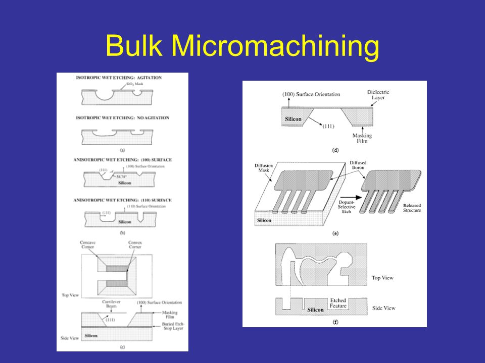
Bulk Micromachining “Bulk” means substrate Make a structure on top of the substrate Etch away the substrate underneath the structure Left with a “floating” structure above a well of missing substrate Key process in creating MEMS

12
Bulk Micromachining

14
Surface Micromachining Often a layer will be deposited (usually an oxide) with the intention of removing it later –“Sacrificial Layer” This allows “floating” structures to be created on top of the substrate without machining the substrate
 with the intention of removing it later – Sacrificial Layer This allows floating structures to be created on top of the substrate without machining the substrate")
15
Surface Micromachining

16
MEMS Examples

17
Photoresist Application Exposure/ Developing Deposition/ Growth or Etching Photoresist Etching Building Devices

18
Photoresist Removal When photoresist is exposed, some of it is washed away with developer revealing the mask pattern Some process is done to the remaining pattern –Deposition, growth, etching… Once that step is done, the remaining hardened photoresist must be removed: –Photoresist Etching

19
Photoresist Removal The hardened photoresist is etched away A wet etch is used to minimize surface damage PECVD methods can be used with O 2 gas, but usually only one wafer at a time –ASHING

20
Plasma Process Control Optical Emission Spectroscopy –Look at the wavelengths and intensities coming out of the plasma Interferometry –Shine a laser onto the substrate and measure the phase changes Mass Spectroscopy –Measures the types and energies of ions present in the plasma Electrical Measurements –Measure the power output of the generator

21
Chemo-Mechanical Polishing Every time a new layer is added to the substrate, it becomes uneven over the surface –Lumpy Even if you deposit a layer of oxide to even things out it’s still lumpy CMP allows planarization of the wafer before the next layer is added Very important in metal layers to have predictable line resistances

22
Chemo-Mechanical Polishing Wafer is held face down in a “carrier” Polishing pad is underneath “Slurry” is sprayed between the two –Slurry would be a somewhat chemically reactive solution with bits of hard material in it to scrape and eat away at the surface The wafer and pad are pushed together and spun around to ensure even wearing of the surface

23
Chemo-Mechanical Polishing

25
CMP is a relatively rough process and if it’s not done very carefully it can cause defects Tight process control must be used Wafers must be cleaned once they’ve been through CMP

26
Chemo-Mechanical Polishing Without CMP, the divisions between metal layers would be wobbly (lumpy) instead of straight
 instead of straight")
27
Chemo-Mechanical Polishing

28
Thank You! This presentation will be available on the web.

Similar presentations

>")

 Grey=Si, Blue=Silicon Dioxide, Red=Photoresist, Purple= Phosphorus.>")


