Download presentation
Presentation is loading. Please wait.

1
CMOS Inverter Layout P-well mask (dark field) Active (clear field)
DD Active (clear field) PMOS W/L=9l/2l Gate (clear field) Note body contacts: p-well to GND n-substrate to VDD Select mask (dark field & clear field) NMOS W/L=3l/2l Contact (dark field) GND Metal (clear field)
 PMOS. W/L=9l/2l. Gate. (clear field) Note body contacts: p-well to GND. n-substrate to VDD. Select mask. (dark field & clear field) NMOS. W/L=3l/2l. Contact. (dark field) GND. Metal. (clear field)")
2
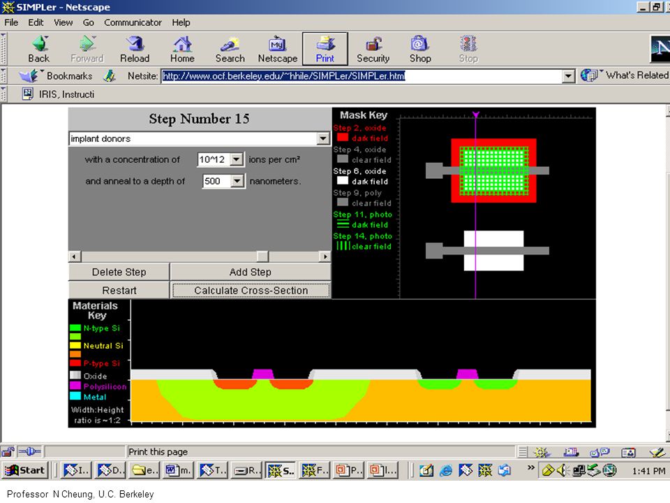
Visualizing Layouts and Cross-Sections with SIMPLer
SIMPL is a CAD tool created by Prof. Neureuther’s group allows IC designers to visualize device cross-sections corresponding to a fabrication process and physical layout. A Berkeley undergraduate student, Harlan Hile, created a mini-version of SIMPL (called SIMPLer) for EE40. It’s a JAVA program -> can be run on any computer, as well as on a web server. A 3D version SIMPL-GL can be accessed at
 for EE40. It’s a JAVA program -> can be run on any computer, as well as on a web server. A 3D version SIMPL-GL can be accessed at.")
8
Twin Well + STI CMOS Process
Define active areas; etch Si trenches Fill trenches (deposit SiO2 then CMP) Form wells (implantation + thermal anneal) Grow gate oxide Deposit poly-Si and pattern gate electrodes Implant source/drain and body-contact regions Activate dopants (thermal anneal) Deposit insulating layer (SiO2); planarize (CMP) Open contact holes; deposit & pattern metal layer
 Form wells (implantation + thermal anneal) Grow gate oxide. Deposit poly-Si and pattern gate electrodes. Implant source/drain and body-contact regions. Activate dopants (thermal anneal) Deposit insulating layer (SiO2); planarize (CMP) Open contact holes; deposit & pattern metal layer.")
9
3D view of a CMOS inverter after contact etch.
9

10
Well Engineering P-tub N-tub Twin Tub 10

11
Twin Well CMOS Process Flow
11

12
Retrograde Well - formed by high energy (>200keV) implantation C(x)
Conventional well (depth and profile controlled by diffusion drive-in) Retrograde well (depth and profile controlled by implantation energy and dose) x 12
 Retrograde well (depth and profile. controlled by implantation. energy and dose) x. 12.")
13
Conventional vs Retrograde Well
Very low thermal budget for well formation (no need for diffusion drive-in) 2) Retrograde Well is formed AFTER field oxidation small lateral diffusion and localized high conc under FOX 13
 2) Retrograde Well is formed AFTER field oxidation. small lateral diffusion and localized high conc under FOX. 13.")
14
Example: Formation of Channel Stop and Retrograde Well
in a single step Retrograde well Channel stop 14

15
Multiple Implants for Well Engineering
15

16
Channel Engineering Shallow Oxide Trench Isolation
N Cheung EE243 Sp2010 Lec 1

17
Generic Silicon-on-Insulator (SOI) CMOS Process Flow
17

18
SOI Process Flow (continued)
18

19
Self-Aligned Channel V-gate by Optical Lithography
(SALVO) Process Smallest feature printable by lithography Normal S/D implant Oxide spacer poly-Si gate CVD oxide CVD oxide n+ n+ n+ n+ SiO2 Thermal gate oxide Angled Implant n+ pocket TiSi2 * Sub-50nm channels 19
 Process. Smallest feature. printable by. lithography. Normal. S/D implant. Oxide spacer. poly-Si gate. CVD oxide. CVD oxide. n+ n+ n+ n+ SiO2. Thermal. gate oxide. Angled. Implant. n+ pocket. TiSi2. * Sub-50nm channels. 19.")
20
SALVO Process Flow or See Homework Problem Chang et al, IEDM 2000 20

21
SUMMARY OF IC PROCESS INTEGRATION MODULE
Self aligned techniques: channel stop, Source/Drain, LDD, SALICIDE How to read process flow descriptions and cross-sections Generic NMOS Process with LOCOS Generic CMOS Process with LOCOS and single well Modified Processes: Shallow Trench Isolation (STI), Twin Wells, Retrograde Well, SOI CMOS 21
, Twin Wells, Retrograde Well, SOI CMOS. 21.")
Similar presentations


 Absolute-Value Design Rules * Use absolute distances (2) -based.>")


 Sherief Reda Division of Engineering, Brown University Spring 2007 [sources: Sedra/Prentice Hall, Saint/McGrawHill,>")


