Download presentation
Presentation is loading. Please wait.

1
Optical properties of infrared emission quaternary InGaAsP epilayers Y. C. Lee a,b, J. L. Shen a, and W. Y. Uen b a. Department of Computer Science and Information Engineering, Tung Nan Institute of Technology, Taipei, Taiwan, R.O.C. b. Department of Physics, Chung Yuan Christian University c. Department of electronic, Chung Yuan Christian University

2
Long wavelength (1.3 ~1.55μm) emission quaternary InGaAsP semiconductor have been studied extensively because of their potential application to optical fiber communication system. The growth methods of InGaAsP layers: a. MBE (molecular beam epitaxy) b. LPE (liquid phase epitaxy) Introduction
 b. LPE (liquid phase epitaxy) Introduction.")
3
Introduce to MBE

4
molecular source shutter Substrate Buffer

5
Introduce to LPE

6
Introduction Liquid Phase Epitaxy ( LPE ) growth process has the unintentional residual impurity from the melt, substrate, source materials and growth ambient. Doping rare-earth elements into semiconductor is the interest method to reduce the residual impurities (S, Se, Si, C, Te, O, etc.) in the LPE growth. Optoelectronic Lab.
 in the LPE growth. Optoelectronic Lab..")
7
Introduction The rare-earth elements as the gettering agent have been reduce the impurities which as donors in semiconductor. The rare-earth elements are insoluble in the solvent used in LPE growth and they are not incorporated into the grown epitaxial layer. Optoelectronic Lab.

8
Introduction There have been many reports describing the effects of the rare-earth doping on semiconductors with Er, Yb, and Gd elements but few describing about Ho. In this work, we present the influence of Ho and Nd elements doped into quaternary InGaAsP layers by the PL 、 PC 、 CER and Raman measurements. Optoelectronic Lab.

9
Samples Profile Optoelectronic Lab.

10
Photoluminescence Measurement Optoelectronic Lab. Monochromator

11
Photoluminescence K-Space C.B. V.B. luminescence Laser (E > E g ) electron recombination electron hole electron
 electron recombination electron hole electron.")
12
Results and Discussion 12 K PL spectra of LPE- grown InGaAsP layers as a function of doping amount of the Ho elements: (a) undoped (b) 0.017 wt % (c) 0.025 wt % (d) 0.075 wt % (e) 0.110 wt % (f) 0.150 wt % Optoelectronic Lab.
 undoped (b) wt % (c) wt % (d) wt % (e) wt % (f) wt % Optoelectronic Lab.")
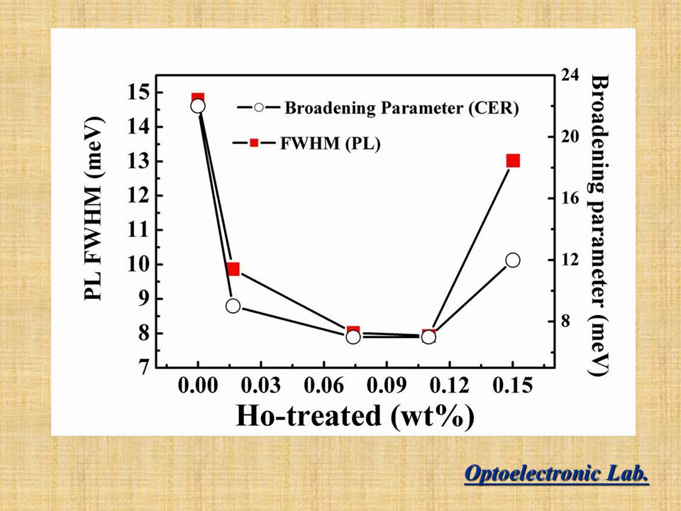
13
Results and Discussion The FWHM of the photoluminescence extracted as a function of the doping amounts of the Ho element. Optoelectronic Lab. Larger lattice mismatch [M. C. Wu, J. Appl. Phys 71,456 (1992)]
].")
14
Photoconductivity Measurement Optoelectronic Lab.

15
Results and Discussion

16
Optoelectronic Lab. Band tail Theroy

17
Three main possible mechanisms For explaining the band tail 1.Phonon-assisted transition: The slop of the band edge is not strong dependent on the temperature. 2.Alloy disorder: With the evaluation of asymmetric broadening of Raman signals, the alloy disorder does not change owing to the Ho doping. 3.Impurity disorder: From the above argument, We suggest that the impurity are responsible for the presence of the Urbach tail in our samples. Results and Discussion

18
Urbach expreesion: α= α 0 exp (hν/E 0 ) α : the absorption coefficient α 0 : constant E 0 : the Urbach energy [F. Urbach, Phys. Rev. 92, 1324 (1953)] Optoelectronic Lab. The value of E 0 which represents the distribution of the tail states extending into the band gap and can be correlated with impurity concentrations on the sample.
] Optoelectronic Lab. The value of E 0 which represents the distribution of the tail states extending into the band gap and can be correlated with impurity concentrations on the sample..")
19
Results and Discussion The PC spectra of the Ho-doped sample as a function of the doping amount of the Ho elements: (a) undoped (b) 0.017 wt % (c) 0.025 wt % (d) 0.075 wt % (e) 0.110 wt % (f) 0.150 wt% The open circles show the fit to the absorption tail. Optoelectronic Lab.

20
Results and Discussion The values of Urbach energy E 0 as a function of Ho wt %. Optoelectronic Lab.

21
Results and Discussion Values of PL FWHM and Urbach energies of InGaAsP layers with various amount of Ho elements Optoelectronic Lab.

22
Contactless Electronrefelectanc Measurement Optoelectronic Lab.

23
Third-derivative Functional Fit (TDFF) E : the incident photon energy E o : the interband transition energy Γ : the broadening parameter C : the amplitude θ : the phase m : 2.5 for bulk materials
 E : the incident photon energy E o : the interband transition energy Γ : the broadening parameter C : the amplitude θ : the phase m : 2.5 for bulk materials")
24
Results and Discussion Optoelectronic Lab. 14-K CER spectra of InGaAsP epilayers as a function of doping amount of the Ho elements: (a) undoped (b) 0.017 wt % (c) 0.075 wt % (d) 0.110 wt % (e) 0.150 wt %. The open circles are fits to a TDFF model.
 undoped (b) wt % (c) wt % (d) wt % (e) wt %. The open circles are fits to a TDFF model..")
25
Results and Discussion Values of interband transition, broadening parameter, phase in the fitting of CER lineshapes Optoelectronic Lab.

27
Micro-Raman measurement Monochromator Optoelectronic Lab.

28
Results and Discussion [ P.Parayanthal and Fred H. Pollak,Phys. Rev. Lett. 52,1822 (1983) ] The Raman peaks have an asymmetric lineshape, which can be analyzed by a spatial correlation (SC) model. The alloying or any imperfection in semiconductors may destroy the configurational symmetry and break down the q= 0 momentum selection rule. The spatial correlation function of phonon hence become finite and the Raman spectrum reveals an asymmetric line shape (Γ a >Γ b ).
 ] The Raman peaks have an asymmetric lineshape, which can be analyzed by a spatial correlation (SC) model. The alloying or any imperfection in semiconductors may destroy the configurational symmetry and break down the q= 0 momentum selection rule. The spatial correlation function of phonon hence become finite and the Raman spectrum reveals an asymmetric line shape (Γ a >Γ b )..")
29
Results and Discussion The Raman peak (InAs-like LO mode) have an asymmetric line shape, which can be fitted by : The asymmetric ratio (Γ a /Γ b ) as a function of Ho amounts are almost unchanged the alloy disorder or the structural imperfection in InGaAsP layers is not affected by the Ho doping
 have an asymmetric line shape, which can be fitted by : The asymmetric ratio (Γ a /Γ b ) as a function of Ho amounts are almost unchanged the alloy disorder or the structural imperfection in InGaAsP layers is not affected by the Ho doping")
30
Conclusion ( Ⅰ ) 1.The FWHM of PL peak has been found to reduce as the doping of Ho elements increases from 0 to 0.11 wt %. The narrowest value of the FWHM of PL peak is 7.93 meV with Ho of 0.11 wt%, which is smaller by about 46 % than that of the undoped InGaAsP and better than previous reports on similar composition layers. 2.It is found that the Urbach energy decreases as the Ho doping increases except the sample with 0.1502 wt% Ho-doped, indicating the Ho doping leads to the decrease of impurity concentrations. Published in Solid-State Commun. 120, 501 (2001)
.")
31
3.The broadening parameter of contactless electrorefelectasnce spectra has been found to decrease as a function of the Ho-doped increased. 4.We demonstrate that the rare-earth element can be an efficient gettering agent for LPE- grown InGaAsP layers and improves the quality of LPE-grown epilayers. Conclusion ( Ⅱ ) Published in Phys. Stat. Sol. (a) 200, 439 (2003)
 Published in Phys. Stat. Sol. (a) 200, 439 (2003).")
32
Conclusion ( Ⅲ ) 1.The Raman line shapes of the Ho-doped InGaAsP epilayers are asymmetric. Based on the spatial correlation model, it is found the asymmetric ratio and correlation length of the Raman signals are not influenced by the rare-earth doping. 2.This result suggests that no large amounts of the rare- earth elements are incorporated into the epilayers during purification although the residual impurities can be greatly reduced. Optoelectronic Lab. Published in Solid-State Commun. 129, 47 (2004)
.")
Similar presentations
, S.-K. Lee 1), D. Hongxing 2), Z. Chen 2),>")


, high efficiency (up to 40%), tuneable lasers, which have.>")
 Low dimensional materials: Quantum wells,>")

