Download presentation
1
Electron Microscopy for Catalyst Characterization Dr. King Lun Yeung Department of Chemical Engineering Hong Kong University of Science and Technology CENG 511 Lecture 3

2
Electron-Specimen Interaction e-e- e-e- e-e- backscattered e - elemental contrast secondary e - surface topography Primary or unscattered e - projected sample image transmission electron microscopy http://www.jeol.com/sem_gde/imgchng.html http://www.unl.edu/CMRAcfem/ http://www.ou.edu/research/electron/www-vl/ http://www.mwrn.com/guide/electron_microscopy/microscope.htm

3
Specimen Interaction Volume (V i ) Auger secondary e- backscattered e- K X-ray L X-ray increasing depth surface information bulk information V i when accelerating V i when incident angle V i when atomic number
 Auger secondary e- backscattered e- K X-ray L X-ray increasing depth surface information bulk information V i when accelerating V i when incident angle V i when atomic number ")
4
Electron-Specimen Interaction Backscattered electrons Topography (A-B) Composition (A+B)
 Composition (A+B)")
5
Electron-Specimen Interaction Secondary electrons

6
Electron-Specimen Interaction Ugly BUGS

7
Electron-Specimen Interaction Surface Topography of Catalyst-related Materials

8
Electron-Specimen Interaction Primary or unscattered electrons diamond gold TEM

9
Electron-Specimen Interaction e-e- e-e- e-e- X-rays bulk elemental composition Auger electrons surface elemental composition Cathodaluminescence band-gap energy, electronic property http://jan.ucc.nau.edu/~wittke/Microprobe/ProbeNotes.html

10
Electron-Specimen Interaction Cathodaluminescence

11
Electron-Specimen Interaction Cathodaluminescence Ion implanted silicon patterns

12
Electron-Specimen Interaction X-rays Sampling volume for X-ray X-rays Si(Li) detector
 detector")
13
Electron-Specimen Interaction Si(Li) Detector E Ne - PULSE 1 PULSE 2
 Detector E Ne - PULSE 1 PULSE 2")
14
Electron-Specimen Interaction Si(Li) Detector Window
 Detector Window")
15
Electron-Specimen Interaction Energy Dispersive X-ray Spectroscopy Si (bright)Al (bright)
Al (bright)")
16
Electron-Specimen Interaction http://jan.ucc.nau.edu/~wittke/Microprobe/Interact.html#Aug Auger Electron WKWK WLWL WMWM WNWN WGWG KK KK LL Auger e - or Auger e - Z

17
Scanning Electron Microscopy specimen Electron gun

18
SEM - Electron Gun

19
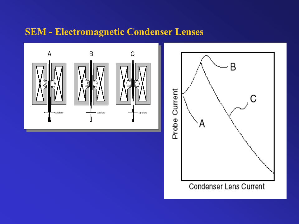
SEM - Electromagnetic Condenser Lenses

21
Figure C-8. The light optics (4) and scanning coils (1) are located inside the minicoil probe- forming lens (2) at the base of the electron column. The pole piece (7) is one solid piece of metal and protects the sample from stray magnetic fields. The x-ray beams (3) are collimated by small apertures (6), and pass through an electron trap (5) that prevents backscattered electrons from entering the x-ray pectrometers. SEM - Objective Len
 and scanning coils (1) are located inside the minicoil probe- forming lens (2) at the base of the electron column. The pole piece (7) is one solid piece of metal and protects the sample from stray magnetic fields. The x-ray beams (3) are collimated by small apertures (6), and pass through an electron trap (5) that prevents backscattered electrons from entering the x-ray pectrometers. SEM - Objective Len.")
22
SEM - Electron Probe

23
SEM - Image Formation-1

24
SEM - Image Formation-2

25
Scanning Electron Microscopy high voltage low voltage Effect of accelerating voltage http://www.jeol.com/sem_gde/imgchng.html

26
Scanning Electron Microscopy Effect of accelerating voltage http://www.jeol.com/sem_gde/imgchng.html

27
Scanning Electron Microscopy Effect of beam current and spot size http://www.jeol.com/sem_gde/imgchng.html

28
Scanning Electron Microscopy Effect of accelerating voltage http://www.jeol.com/sem_gde/imgchng.html

29
Scanning Electron Microscopy Effect of accelerating voltage http://www.jeol.com/sem_gde/imgchng.html

30
Scanning Electron Microscopy Incorrect alignment of objective aperture http://www.jeol.com/sem_gde/imgchng.html

31
Scanning Electron Microscopy Effect of specimen tilt http://www.jeol.com/sem_gde/imgchng.html Stereo microscopy

32
Scanning Electron Microscopy Effect of accelerating voltage http://www.jeol.com/sem_gde/imgchng.html (1) (2) (3)
 (2) (3)")
33
Scanning Electron Microscopy Contrast and brightness http://www.jeol.com/sem_gde/imgchng.html

34
Scanning Electron Microscopy Astigmatism http://www.jeol.com/sem_gde/imgchng.html

35
Scanning Electron Microscopy Sample charging http://www.jeol.com/sem_gde/imgchng.html

36
Scanning Electron Microscopy Preventing charging by thin film coating http://www.jeol.com/sem_gde/imgchng.html

37
Scanning Electron Microscopy Electron beam damages and contamination http://www.jeol.com/sem_gde/imgchng.html Carbon contaminant deposited by electron beam Electron beam damage on a fly’s compound eye

38
Scanning Electron Microscopy Sources of image distortions http://www.jeol.com/sem_gde/imgchng.html

39
Scanning Electron Microscopy Influence of external disturbances http://www.jeol.com/sem_gde/imgchng.html

40
Scanning Electron Microscopy Importance of sample preparation http://www.jeol.com/sem_gde/imgchng.html

41
Electron-Specimen Interaction e-e- e-e- e-e- backscattered e - elemental contrast secondary e - surface topography Primary or unscattered e - projected sample image transmission electron microscopy http://www.jeol.com/sem_gde/imgchng.html http://www.unl.edu/CMRAcfem/ http://www.ou.edu/research/electron/www-vl/ http://www.mwrn.com/guide/electron_microscopy/microscope.htm

42
Electron-Specimen Interaction Principle of E. M. lithography Polymer resist Substrate

43
Electron Beam Lithography Micropatterning and Microfabrication PMMA resist E-beam develop resist selectively etch substrate http://www.cnf.cornell.edu/SPIEBook/spie5.htm#2.5.3.1

44
Microfabricated Catalysts deposit alternate layers of catalyst and inert micropattern and etch undercut and remove 50 nm nickel, 50 nm SiO 2

45
Supported Catalysts Metal supported on metal oxide Coarsening

46
Microfabricated Catalysts Zeolite micropatterned catalysts Zeolite Grids (200)/(020)(101) Zeolite Grids
/(020)(101) Zeolite Grids")
47
Electron-Specimen Interaction Electron beam Thin sample Unscattered electrons

48
Different Types of Electron Microscopy SEM TEM Ultra-TEM HREM

49
Transmission Electron Microscopy Au/SiO 2 http://www.mwrn.com/guide.htm http://www.hei.org/research/depts/aemi/micro.htm

50
Electron-Specimen Interaction

51
Transmission Electron Microscopy Au

52
Transmission Electron Microscopy Primary or unscattered electrons diamond gold TEM http://em-outreach.sdsc.edu/web-course

53
Transmission Electron Microscopy Catalyst particle size distribution

54
Transmission Electron Microscopy Catalyst particle shape and morphology

55
Particle Morphology Selected zone dark field imaging (SZDF) ? ?
")
56
Particle Morphology Selected zone dark field imaging (SZDF) (100) (110)
 (100) (110)")
57
Particle Morphology Weak beam dark field (WBDF)
 ")
58
Particle Morphology SZDF and WBDF techniques

59
Electron-Specimen Interaction

60
Transmission Electron Microscopy Distribution of crystallographic planes

61
Electron-Specimen Interaction

62
High Resolution Electron Microscopy http://bnlstb.bio.bnl.gov/biodocs/stem/interactive.htmlx Bismuth molybdates (Bi 2 Mo 3 O 12 - )
")
63
High Resolution Electron Microscopy Bismuth molybdates (Bi 2 MoO 6 - )
")
64
High Resolution Electron Microscopy Platinum on Alumina hydrogen Hydrogen sulfide

65
High Resolution Electron Microscopy 2 x 1 reconstruction of (110) surface of Au particle
 surface of Au particle")
66
High Resolution Electron Microscopy Rh/SiO 2 Reduced Oxidized

67
High Resolution Electron Microscopy Rh particles

68
High Resolution Electron Microscopy Electron-beam induced reduction of RuCl 3 on MgO

69
High Resolution Electron Microscopy Hydrogen reduced Rhodium-TiO 2

70
Electron-Specimen Interaction


 1.Overview. 2.Ion source and optics. 3.Ion-solid interaction, damage. 4.Scanning ion beam imaging. ECE 730: Fabrication in the nanoscale:>")

 Resolution strongly dependent of wavelength: –electron microscope: about.>")


>")


>")


 Transmission Electron Microscope (TEM) Atomic Force.>")