Download presentation
Presentation is loading. Please wait.

1
*Sequential logic circuit:. It is consist of logic getes and storge element (memory element )the o\p depend of i\p and the past i\p the flip flop circuit sitis the basic desigen of it. The system whose behavior can be defined form the know lodge of its signal at descrete of time.. The system whose behavior can be defined form the know lodge of its signal at descrete of time..
the o\p depend of i\p and the past i\p the flip flop circuit sitis the basic desigen of it. The system whose behavior can be defined form the know lodge of its signal at descrete of time.. The system whose behavior can be defined form the know lodge of its signal at descrete of time...")
2
The storge element(memory)use in clocked sequential cct are called llip flop… Is binary storge device capuble of storge one bit of information. Asequential cct my use many flip flops to store as many bits as no necessary,,

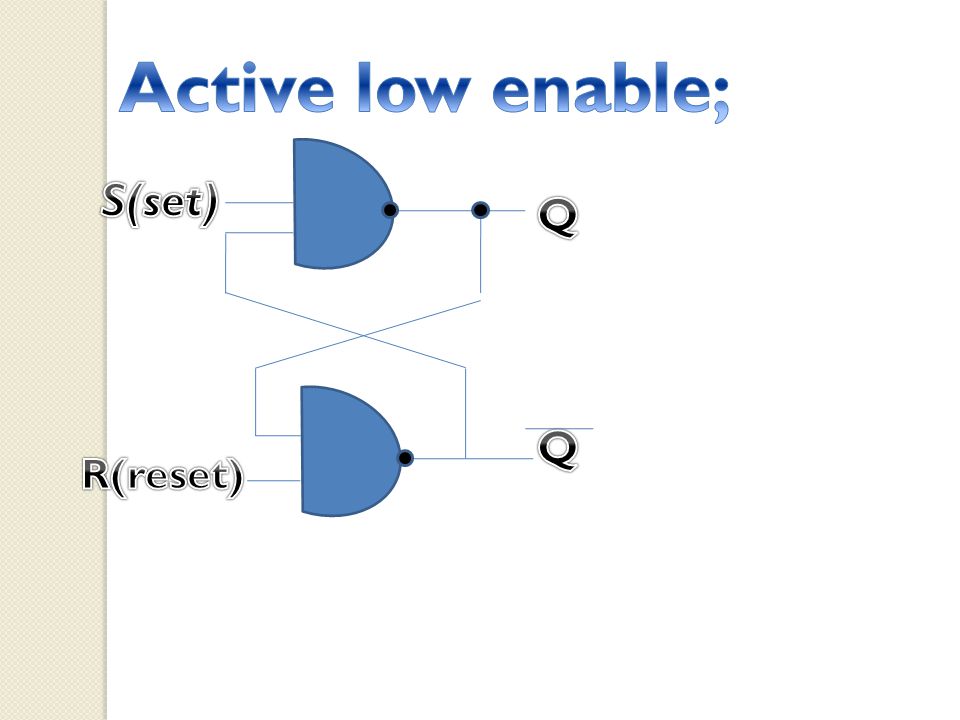
5
It’s the circuit with tow cross coupled no rgetes or two cross-coupled NAND getes two I\ps labeled S (set) and R (reset),and it,s basic cct from which all flip-flop are constructed.. Active high enable…

6
stateso\pi\ps No changeQRS Q00 Reset010 Sets101 Not allowedX11 Truth table S-R latch of high enable

7
RS latch M of high enable Sequent clock=synchsequet cct=clock seque cct+ Storget clock=flip flop

8
den 00 11 11 No change Q =0 reset Q =1 set Next of a “block diagram D latch”

10
QRS 100 110 001 011

11
Types of flip flop... *it is construction of tow dlatches and inverter. The first latch is called the(master)and the second called the(slave)
and the second called the(slave).")
12
D cl k D Q Q Positv edge Negativ edge Positv edge

13
statesQ(t+t)D Reset set00 11 J Q Qclck K D
D Reset set00 11 J Q Qclck K D")
14
statesQ(t+t)KJ No changQ00 Reset010 Set101 complementQ11
KJ No changQ00 Reset010 Set101 complementQ11")
15
Q Q S R

Similar presentations