Download presentation
Presentation is loading. Please wait.

1
Deposition and Etching of Thin Films Nathaniel J. C. Libatique, Ph.D. nlibatique@gmail.com

2
Sze, Semiconductor Devices, John Wiley and Sons Process Steps Start with polished wafers of chosen and crystal orientation Films: epitaxial, thermal oxides, polysilicon, dielectrics, metals Doping: via diffusion or ion implantation Lithography: shadow masked or projection Etching: Wet and Dry Sequential Mask Transfer Stepper Iteration

3
Starting Materials Quartzite + carbon sources (coal, coke, wood chips) SiC(solid) + SiO 2 (solid) Si(solid) + SiO(gas) + CO (gas) provides metallurgical grade silicon (98%) Pulverize silicon and treat with HCl to produce trichlorosilane Si(solid) + 3 HCl(gas) 300oC SiHCl 3 (gas) + H 2 (gas) trichlorosilane liquid at RT. Fractional distillation. Purified trichlorosilane in hydrogen reduction reaction SiHCl3(gas) + H2(gas) Si(solid) + 3HCl(gas) EGS (electronic grade Si) is produced. Ppb impurities. Poly. (Elemental Ga and As are the starting materials for GaAs poly) http://csmres.jmu.edu/geollab/Fichter/MetaRx/Rocks/quartzite1.html
 + H2(gas) Si(solid) + 3HCl(gas) EGS (electronic grade Si) is produced. Ppb impurities. Poly. (Elemental Ga and As are the starting materials for GaAs poly)")
4
Sze, Semiconductor Devices, John Wiley and Sons Single Crystal Furnace Pulling Mechanism Ambient Control rotation mechanism, heating elements and power supply, seed holder, rotation mechanism, Ar gas, gas flow, exhaust, temperature, Si diameter, pull rate, rotation speed

5
Wafer Flats Grind to fixed diameter, edge grind for auto placement algos Secondary flats reveal conductivity and type Slice determines orientation, thickness, taper (t variation), bow (center to edge) Lap with Al 2 O 3 and glycerine, flatness within 2 m Etch and polish Sze, Semiconductor Devices, John Wiley and Sons
, bow (center to edge) Lap with Al 2 O 3 and glycerine, flatness within 2 m Etch and polish Sze, Semiconductor Devices, John Wiley and Sons")
6
Deposition Techniques Thermal Oxidation Evaporation: Thermal & E-Beam Sputtering Vapor Phase Epitaxy Molecular Beam Epitaxy

7
www.cnfusers.cornell.edu/ Thermal Oxidation Many films deposited on semiconductors Native film advantages: - no deposition reqrd - relatively pure - excellent interface -device passivation

8
Silicon Dioxide SiO 2 on Si under fluorescent lighting Native Oxide = 15 to 20 Ang. Si + O 2 SiO 2 ; dry Si + 2H 2 O SiO 2 +2 H 2 ; wet Wet Oxidation: H 2 rapid diff’n Oxide layer 2.7 times thickness of consumed silicon

9
Thermal Evaporation Electron Beam Evaporation gun A System Controller, Power Supply Crucibles for the evaporation material, Materials for Evaporation Material to be coated PLUS Substrates < 100 C High deposition rate Simple procedure MINUS Metals Poor layer adhesion Uneven or structured surfaces 100 meV Energies

10
Sputtering 1 to 20 eV Energies better adhesion Oxides, ceramics, alloys, semiconductors, glasses

11
CVD AX(gas) + BY(gas) AB(solid) + XY(gas) SiH 4 + 2 N 2 O SiO 2 + 2N 2 + 2H 2 SiH 4 + NH 3 Si x N y H z + H 2
 + BY(gas) AB(solid) + XY(gas) SiH N 2 O SiO 2 + 2N 2 + 2H 2 SiH 4 + NH 3 Si x N y H z + H 2")
12
LPCVD

13
Separate effusion chambers (pyrolitic boron nitride) Ultra-high vacuum Arsenic overpressure E-Gun for Si Sze, Semiconductor Devices, John Wiley and Sons Molecular Beam Epitaxy 5 to 30 cm
 Ultra-high vacuum Arsenic overpressure E-Gun for Si Sze, Semiconductor Devices, John Wiley and Sons Molecular Beam Epitaxy 5 to 30 cm")
14
Mean Free Path d c S = Collision cross section = r 2 n particles in a volume V c dt S V One collision only if (n/V) r 2 c dt = [(n/V) r 2 ] -1
![Mean Free Path d c S = Collision cross section = r 2 n particles in a volume V c dt S V One collision only if (n/V) r 2 c dt = [(n/V) r 2 ] -1](http://images.slideplayer.com/13/3715597/slides/slide_14.jpg "Mean Free Path d c S = Collision cross section = r 2 n particles in a volume V c dt S V One collision only if (n/V) r 2 c dt = [(n/V) r 2 ] -1")
15
Ultra-High Vacuum Required = [(n/V) r 2 2 0.5 ] -1 = kT/ (2 0.5 r 2 P) P = nkT/V At room temperature cm = 5 x 10 -3 / P (in Torr) Typical value, 3 Angstrom for d, so about 0.5 x 10 3 cm for partial pressures of 10 -5 Torr
![Ultra-High Vacuum Required = [(n/V) r ] -1 = kT/ (2 0.5 r 2 P) P = nkT/V At room temperature cm = 5 x / P (in Torr) Typical value, 3 Angstrom for d, so about 0.5 x 10 3 cm for partial pressures of Torr](http://images.slideplayer.com/13/3715597/slides/slide_15.jpg "Ultra-High Vacuum Required = [(n/V) r ] -1 = kT/ (2 0.5 r 2 P) P = nkT/V At room temperature cm = 5 x / P (in Torr) Typical value, 3 Angstrom for d, so about 0.5 x 10 3 cm for partial pressures of Torr")
16
Nucleation and Growth Incident Flux Surface diffusion until attachment Desorption, higher probability for crystals adsorbed on a low binding energy site Binding energies also function of surface, slower growth rate than in silicon Surface preparation is key

17
Binding Energies 1 nearest neighbor, 2 second nearest neighbors 1, 2, 3, 4 4, 6, 6, 8 Ghandi, VLSI Fabrication Principles, 2 nd Ed., John Wiley and Sons

18
Special Considerations Off axis growth, say 2 to 4 degrees, series of steps and kinks are introduced Elevated substrate temperatures increase surface diffusion (E a,surface is 25% to 50% E a,bulk ) Si (111) planes more easily stacked than (100), plane to plane distance is 57% of (111), better morphology GaAs special.
 Si (111) planes more easily stacked than (100), plane to plane distance is 57% of (111), better morphology GaAs special.")
19
Ghandi, VLSI Fabrication Principles, 2 nd Ed., John Wiley and Sons Successive Layers two dangling bonds, alernate Ga and As deposition Double layers separated by a wide spacing. One dangling bond. yy’ signinficantly different from xx’. Significant surface energy change. GaAs

20
Surface Morphology

21
Comparison [Gerlach and Dotzel]
![Comparison [Gerlach and Dotzel]](http://images.slideplayer.com/13/3715597/slides/slide_21.jpg "Comparison [Gerlach and Dotzel]")
22
Etching

23
Si 20.. 40 SiO 2 30.. 40 Au 140 Etch rates in nm/min for ion beam etch (Ar +, 0.5 keV, ion flow at 1 mA/cm ) Al 30 PR AZ 1350 20.. 30 Comparison
 Al 30 PR AZ 1350 Comparison.")
25
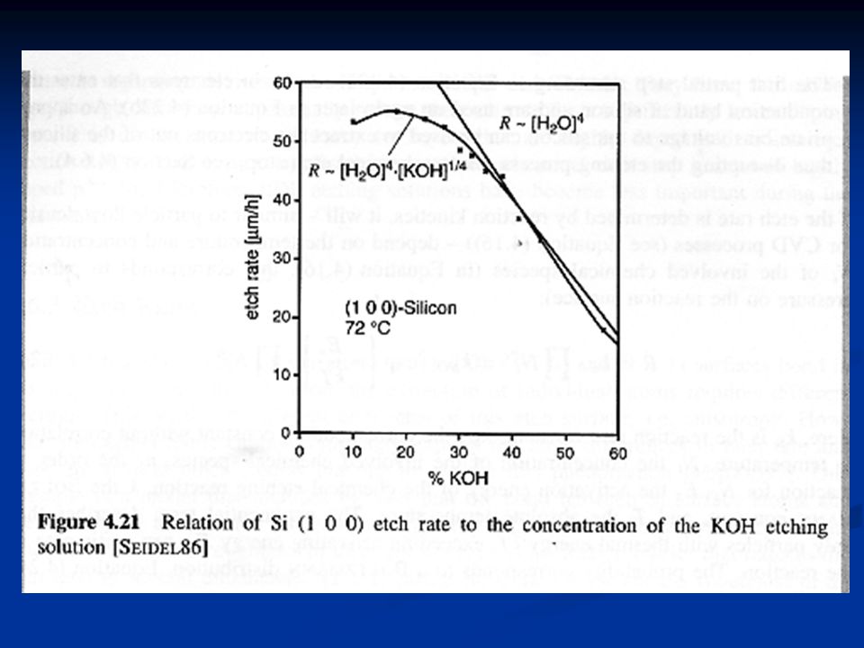
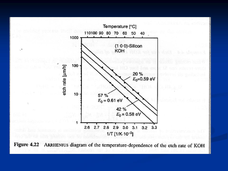
Wet Etch: Anisotropic

33
References G. Gerlach and W. Dotzel, “Introduction to Microsystem Technology, A Guide for Students”, Wiley, ISBN 978-0-470-05861-9 G. Gerlach and W. Dotzel, “Introduction to Microsystem Technology, A Guide for Students”, Wiley, ISBN 978-0-470-05861-9

Similar presentations


>")


>")


