Download presentation
Presentation is loading. Please wait.

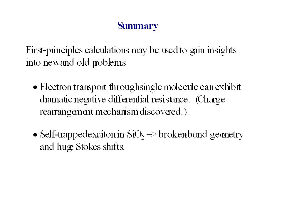
1
Deriving Insights from Computation: Molecular Electronics to Self-trapped Excitons Steven G. Louie Physics Department, UC Berkeley and MSD, LBNL Electron Transport: Self-trapped Excitons: Supported by: NSF and DOE J.-H. Choi Y.-W. Son J. Neaton J. Ihm (Korea) K. Khoo M. Cohen S. Ismail-Beigi (Yale) O1O1 Si 1 Si 2
 K. Khoo M. Cohen S. Ismail-Beigi (Yale) O1O1 Si 1 Si 2.")
2
Molecular Electronics Present approach: Ab initio scattering-state method Other ab initio approaches: NEGF methods -- (e.g., TRANSIESTA, Guo, et al., …) Lippman-Schwinger -- (e.g., di Ventra & Lang, …) Master equation -- (e.g., Gebauer & Car, …) (Electron transport through single molecules, atomic wires, …)
 Lippman-Schwinger -- (e.g., di Ventra & Lang, …) Master equation -- (e.g., Gebauer & Car, …) (Electron transport through single molecules, atomic wires, …)")
3
Example of a Molecular Electronic Device (For a review, see Reed & Chen, 2000) Chen, et al (1999); Rawlett, et al (2002)
 Chen, et al (1999); Rawlett, et al (2002)")
4
Some fundamental issues Open system: infinitely large and aperiodic Out of equilibrium: Chemical potential ill- defined across molecule Nanometer length scales: atomic details of contact and self- consistent electronic structure are important µLµL µRµR Current RR LL V scf = V pp + V Ha + V xc Self-consistent potential

5
Theoretical framework Compute bias-dependent transmission coefficients t Current from transmission of states T(E,V) Formalism for an open, infinite system out of equilibrium capturing the atomic-scale details of the molecular junction Two-terminal geometry with semi-infinite leads R leadConductor r t L lead i
 Formalism for an open, infinite system out of equilibrium capturing the atomic-scale details of the molecular junction Two-terminal geometry with semi-infinite leads R leadConductor r t L lead i")
6
First-principles Scattering-State Approach to Molecular Electronic Devices Choi, Cohen & Louie (2004)
")
7
Closer look at a scattering state Example state propagating from left to right with energy E where, e.g., Transmission matrix Incident L lead state Transmitted R lead state & evanescent waves Reflected L lead state & evanescent waves Conductor C state R leadConductor r t L lead i

8
Conductance of Pt-H 2 junction [1] R.H.M. Smit et al., Nature 419, 906 (2002) Conductance (2e 2 /h) Number of Counts Pt Conductance of single H 2 molecule has been interpreted by break-junction measurements to be close to 1 G 0 = 2e 2 /h Single channel
![Conductance of Pt-H 2 junction [1] R.H.M.](http://images.slideplayer.com/13/3620256/slides/slide_8.jpg "Smit et al., Nature 419, 906 (2002) Conductance (2e 2 /h) Number of Counts Pt Conductance of single H 2 molecule has been interpreted by break-junction measurements to be close to 1 G 0 = 2e 2 /h Single channel.")
9
Pd-H 2 junction: Reduced conductance Pd Increasing H 2 conc. x PdH x 12345 1234512345 Counts Conductance (2e 2 /h) Similar experiments with Pd nanojunctions yields about 0.3-0.5 G 0, a factor of two or three less than Pt.
 Similar experiments with Pd nanojunctions yields about G 0, a factor of two or three less than Pt..")
10
Modeling the junction H—H? [111] Tip—H? Break junction
![Modeling the junction H—H [111] Tip—H Break junction](http://images.slideplayer.com/13/3620256/slides/slide_10.jpg "Modeling the junction H—H [111] Tip—H Break junction")
11
Transmission spectra Resonances Plateau Khoo, Neaton & Louie (2005) G=1.01G 0 G=0.35G 0 EFEF Pt Pd Resonances
 G=1.01G 0 G=0.35G 0 EFEF Pt Pd Resonances")
12
Physical picture EFEF Pt E Pt case Pd case Pd E EFEF Junction states are band-like Scattering is minimal over a range of energies Junction states are resonant Scattering is large and energy dependent JunctionMetal

13
Local electronic structure PtPd Transmission (2e 2 /h) H2H2 Tip atom Bulk atom Pt Local density of states H2H2 Tip atom Bulk atom Pd Khoo, Neaton and Louie (2005)
 H2H2 Tip atom Bulk atom Pt Local density of states H2H2 Tip atom Bulk atom Pd Khoo, Neaton and Louie (2005)")
14
Local electronic structure H2H2 Tip atom Bulk atom H2H2 Tip atom Bulk atom PtPd PtPd Local density of states Transmission (2e 2 /h) Band-like Localized Khoo, Neaton and Louie (2005)
 Band-like Localized Khoo, Neaton and Louie (2005)")
15
Conductance of H 2 nanojunctions Pd / H 2 Pt / H 2 Experiment0.3 - 0.6G 0 1.0G 0 Our work (G 0 = 2e 2 /h) 0.35G 0 (Pd) 0.14G 0 (PdH) 1.01G 0 H 2 nanojunction conductance Strongly lead-dependent: Tip atoms play a key role Closed-shell molecule is a good conductor! Transport properties of small molecules are strongly affected by lead Our calculations characterize conduction in the junction and explain experiment Khoo, Neaton & Louie (2005)
.")
16
Negative Differential Resistance and Lead Geometry Effects

17
Son, Choi, Ihm, Cohen and Louie (2004) Calculated I-V Curve of a Tour Molecular Junction
 Calculated I-V Curve of a Tour Molecular Junction")
18
unoccupied occupied

19
Dominant transmitting state LL UU

20
LL UU

21
Potential Drop across Molecular Junction Potential at 0.6 A above molecular plane

22
Forces in the Photo-Excited State: Self-trapped Exciton

23
Forces in Excited State For many systems, photo-induced structural changes are important – differences between absorption and luminescence – self-trapped excitons – molecular/defect conformation changes – photo-induced desorption Need excited-state forces – structural relaxation – luminescence study – molecular dynamics, etc. GW+BSE approach gives accurate forces in photo- excited state Ismail-Beigi & Louie, Phys. Rev. Lett. 90, 076401 (2003)
.")
24
Excited-state Forces E S = E 0 + Ω S ∂ R E S = ∂ R E 0 + ∂ R Ω S E 0 & ∂ R E 0 : DFT Ω S : GW+BSE Ismail-Beigi & Louie, Phys. Rev. Lett. 90, 076401 (2003).
..")
25
Verification on molecules Ismail-Beigi & Louie, Phys. Rev. Lett. 90, 076401 (2003). Excited-state force methodology Proof of principle: tests on molecules - CO and NH 3 GW-BSE force method works well Forces allow us to efficiently find excited-state energy minima
. Excited-state force methodology Proof of principle: tests on molecules - CO and NH 3 GW-BSE force method works well Forces allow us to efficiently find excited-state energy minima.")
26
SiO 2 ( -quartz): optical properties Oxygen Silicon [1] Ismail-Beigi & Louie (2004) [2] Philipp, Sol. State. Comm. 4 (1966) [1] Emission at ~ 3 eV!
![SiO 2 ( -quartz): optical properties Oxygen Silicon [1] Ismail-Beigi & Louie (2004) [2] Philipp, Sol.](http://images.slideplayer.com/13/3620256/slides/slide_26.jpg "State. Comm. 4 (1966) [1] Emission at ~ 3 eV!.")
27
Self-trapped exciton (STE) in SiO 2 ( -quartz) Triplet STE has ≈ ms and ~ 6 eV Stokes shift [1] [1] e.g. Itoh, Tanimura, & Itoh, J. Phys. C 21 (1988). 1. Start with 18 atom bulk cell 2. Randomly displace atoms by ±0.02 Å 3. Relax triplet exciton state 4. Repeat steps 2&3: same final config. Ismail-Beigi & Louie (2005)
![Self-trapped exciton (STE) in SiO 2 ( -quartz) Triplet STE has ≈ ms and ~ 6 eV Stokes shift [1] [1] e.g.](http://images.slideplayer.com/13/3620256/slides/slide_27.jpg "Itoh, Tanimura, & Itoh, J. Phys. C 21 (1988). 1. Start with 18 atom bulk cell 2. Randomly displace atoms by ±0.02 Å 3. Relax triplet exciton state 4. Repeat steps 2&3: same final config. Ismail-Beigi & Louie (2005).")
28
Structural Distortion from Self-Trapped Exciton in SiO 2 Final configuration: Broken Si-O bond Hole on oxygen Electron on silicon Si in planar sp 2 configuration Ismail-Beigi & Louie (2005) Oxygen Silicon
 Oxygen Silicon")
29
Self-Trap Exciton Geometry Bond (Å)BulkDefect Si 1 -O 1 1.601.97 (+23%) Si 2 -O 1 1.601.68 (+5%) Si 1 -O other 1.601.66 (+4%) AnglesBulkDefect O 1 -Si 1 -O other 109 o ≈ 85 o O other -Si 1 -O other 109 o ≈ 120 o O1O1 Si 1 Si 2
BulkDefect Si 1 -O (+23%) Si 2 -O (+5%) Si 1 -O other (+4%) AnglesBulkDefect O 1 -Si 1 -O other 109 o ≈ 85 o O other -Si 1 -O other 109 o ≈ 120 o O1O1 Si 1 Si 2")
30
Atomic rearrangement for STE No activation barrier!

31
Electron-Hole Wavefunction of Self-Trapped Exciton in SiO 2 Hole probability distribution with electron any where in the crystal Electron probability distribution given the hole is in the colored box

32
Electron & Hole Distributions of Self-Trapped Exciton in SiO 2 Final configuration: Broken Si-O bond Hole on oxygen (brown) Electron on silicon (green) Si in planar sp 2 configuration Ismail-Beigi & Louie, PRL (2005) Oxygen Silicon
 Electron on silicon (green) Si in planar sp 2 configuration Ismail-Beigi & Louie, PRL (2005) Oxygen Silicon")
33
Constrained DFT Calculations Constrained LSDA: DFT with excited occupations Problems: Relaxes back to ideal bulk from random initial displacements: excited-state energy surface incorrectly has a barrier. Large initial distortion needed for STE [1,2] Predicted Stokes shift and STE luminescence energy are very poor to correlate with experiments [1] Song et al., Nucl. Instr. Meth. Phys. Res. B 166-167, 451 (2000). [2] Van Ginhoven and Jonsson, J. Chem. Phys. 118, 6582 (2003).
. [2] Van Ginhoven and Jonsson, J. Chem. Phys. 118, 6582 (2003)..")
34
STE in SiO 2 : Comparison to Experiment Luminescence freq.: T (eV) Stokes shift (eV) Luminescence Pol || z (*) Expt. [1-6] 2.6, 2.74, 2.75, 2.8 6.2-6.4 0.48, 0.65, 0.70 GW+BSE2.856.370.72 CLSDA (forced) 4.122.14---- 1. Tanimura et al., Phys. Rev. Lett. 51, 423 (1983). 2. Tanimura et al., Phys. Rev. B 34, 2933 (1986). 3. Itoh et al., J. Phys. C 21, 4693 (1988). 4. Itoh et al., Phys. Rev. B 39, 11183 (1989). 5. Joosen et al., Appl. Phys. Lett. 61, 2260 (1992). 6. Kalceff & Phillips, Phys. Rev. B 52, 3122 (1996). (*)
 Tanimura et al., Phys. Rev. Lett. 51, 423 (1983). 2. Tanimura et al., Phys. Rev. B 34, 2933 (1986). 3. Itoh et al., J. Phys. C 21, 4693 (1988). 4. Itoh et al., Phys. Rev. B 39, (1989). 5. Joosen et al., Appl. Phys. Lett. 61, 2260 (1992). 6. Kalceff & Phillips, Phys. Rev. B 52, 3122 (1996). (*).")
Similar presentations


![DFT – Practice Simple Molecules & Solids [based on Chapters 5 & 2, Sholl & Steckel] Input files Supercells Molecules Solids.](/14/4353561/big_thumb.jpg "DFT – Practice Simple Molecules & Solids [based on Chapters 5 & 2, Sholl & Steckel] Input files Supercells Molecules Solids.>")


 at 4.2 K it is possible to form atomic.>")
 Tunneling is one of the simplest quantum mechanical process A Laser STM for Molecules Tunneling has transformed surface science. Scanning.>")
 UC Berkeley, Univ.of Illinois, Norfolk State, Northwestern, Purdue, UTEP Quantum Transport in Ultra-scaled.>")