Download presentation
Presentation is loading. Please wait.

1
LWG2 Power Sequence Introduce
Prepared By: Withy He

3
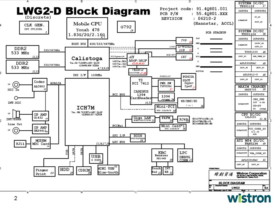
DC-DC Source KBC ICH7-M DCBATOUT 5V_AUX_S5 U4 U5 5V_S5 3D3V_S5 U45
POK U52 U51 1D8V_S3 U44 U74 DDR_VREF_S3 DDR_VREF_S0 U27 5V_S0 3D3V_S0 1D8V_S0 U6 2D5V_S0 U22 U25 VCC_CORE_S0 CPUCORE_ON 1D5V_S0 3D3V_AUX_S5 EN1_5 EN2_3D3 S5_EN S5 S3 S0 PM_SLP_S5# PM_SLP_S3# AD+ MOS BT+ 1D05V_S0 EC_PWRBTN#

4
Charger Circuit MAX8725 Charge Circuit KBC AD+ ACIN ACOK MODE DCBATOUT
CONTROL FEEDBACK ACIN ACOK MODE PKPRES# MAX8725 VCTL ICTL SW BATA_IN# KBC CHG_V_PWM CHG_I_PWN DCBATOUT BT+ DHI DLO CSIP CSIN AD+

5
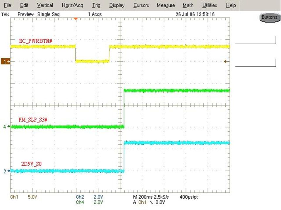
Power On/Reset Step ICH 1.Adapter In: 2.Power On: Adapter In AD+
DCBATOUT 3D3V_AUX_S5 5V_AUX_S5 LP2951 G913 MOS KBC RE144B RTC_AUX_S5 BT+ ICH H8_RESET# 2.Power On: KBC RE144B EC_PWRBTN# S5_EN 5V_S5 TPS51120 3D3V_S5 RSMRST#_TO_KBC PWRBTN#_ICH SB_RSMRST# ICH

6
3.S3: ICH 4.S0: ICH APL5912_KAC TPS51124 PM_SLP_S5# TPS51124 TPS51100
1D8V_S3 DDR_VREF_S3 4.S0: ICH TPS51100 PM_SLP_S3# MOS 3D3V_S0 5V_S0 APL5912_KAC 1D8V_S0 1D5V_S0 APL5332KAC 2D5V_S0 DDR_VREF_S0 TPS51124 1D05V_S0

7
ISL6262 ICH G792 MCH Calistoga CPU Yonah
5.VCC_CORE_S0: TPS51120 POK APL5912_KAC TPS51124 CPUCORE_ON ISL6262 VCC_CORE_S0 6.System Reset: CLK_EN# ISL6262 PGOOD VGATE_PWRGD CPUPWRGD VRMPWRGD ICH PWROK PLTRST1# PCIRST# RESET# G792 HCPURST# MCH Calistoga PWROK RSTIN# PLT_RST1# PCIRST1# GPU DEBUG G.F. LAN HDD/CDROM KBC TI PCI 7412 Power SW H_PWRGD CPU Yonah PWRGOOD H_CPURST# CLK GEN VTT_PWRGD# PWROK

8
Power On/Reset Sequence

Similar presentations


 2. Is this an example of mutually exclusive, overlapping,>")


