Download presentation
Presentation is loading. Please wait.

1
Ch 3. Digital Circuits 3.1 Logic Signals and Gates (When N=1, 2 states)
")
2
–Black-box representation and Truth table shows a logic circuit with input/output and ignores electrical behavior of the circuit Black-box Input Output

3
–AND gate produces 1 : Only if all of its inputs are 1 –OR gate produces 1 : One or more of its inputs are 1 –NOT gate produces an output that is opposite of its input value

4
–NAND Gate : Opposite of an AND gates output –NOR Gate : Opposite of an OR gates output

5
Black-box representationTruth table

6
–Timing diagram show how the circuit might respond to a time-varying pattern of input signals Lag Input Output

7
3.3 CMOS Logic Not expected to occur except during signal transition

8
High resistance : Off Transistor Low resistance : On Transistor NMOS PMOS

10
NMOS PMOS NMOS

11
CMOS inverter

12
On Z=1 On Z=0

13
PMOS NMOS PMOS NMOS PMOS NMOS

14
On Z=0 On Z=1

16
PMOS F NMOS F D F AND -> Series OR -> Parallel PMOS F NMOS F F = F A C A B B D C D

17
AND -> Series OR -> Parallel PMOS F NMOS F

19
Inverter + Inverter

20
NAND + Inverter More Transistors are needed than NAND

22
4x3+2 =14 Transistor 6 Transistor 4 Transistor 16 Transistor

24
4x3+2 =14 Transistor 6 Transistor 4 Transistor 6 Transistor 16 Transistor

25
3.4 Electrical Behavior of CMOS Circuits

27
3.5 CMOS Static Electrical Behavior Noise can be added in signals So, There are noise margins

28
High state Minimum value Low state Maximum value

29
Not CMOS resistive load

32
(TTL load)
")
34
Sink currentSource current

38
Pull-upPull-down

39
No Transition Time in ideal case (20% ~ 80%) (80% ~ 20%)
 (80% ~ 20%)")
40
3.6 CMOS Dynamic Electrical Behavior Both the speed and the power consumption of a CMOS device depend to a large extent on AC device

41
High StateLow State

43
High State

45
50% Ideal case (No rise and fall times) Propagation delay
 Propagation delay")
49
3.7 Other CMOS input and Output Structures

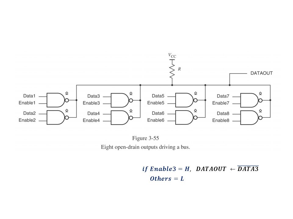
54
Open-drain output requires an external pull-up resistor

55
Increase because R=1.5K Pull-up Resistor

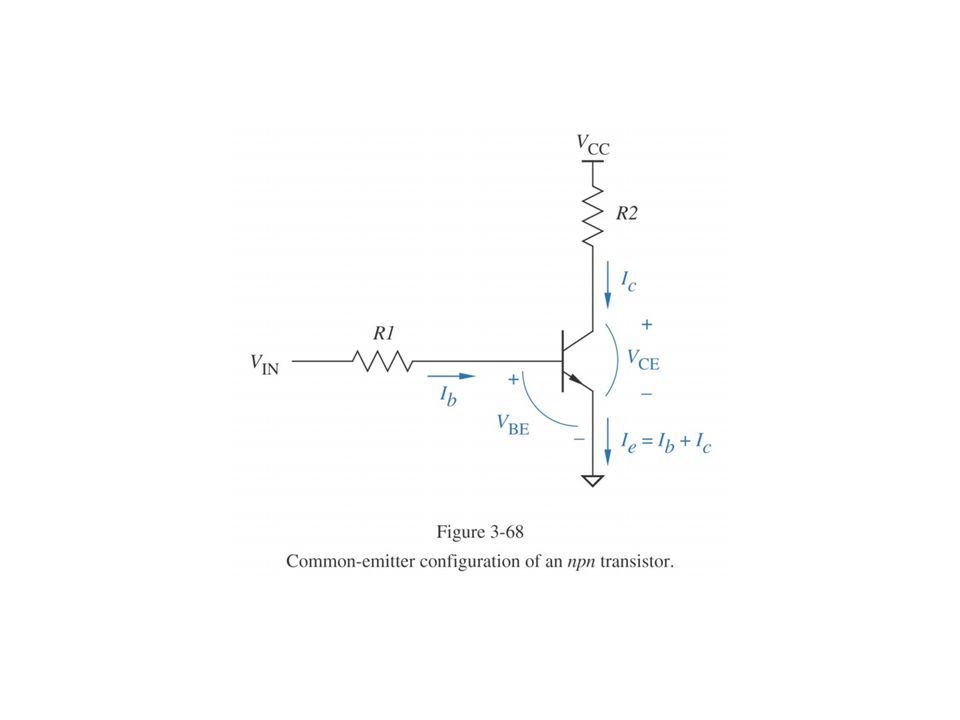
59
X Y W

60
Burn !

61
Low output must sink 0.4mA

62
In high state, typical open-drain outputs have a maximum leakage current 5uA and typical LS-TTL inputs require 20uA of a source current

63
3.8 CMOS Logic Families High-speed CMOSHigh-speed CMOS, TTL compatible

69
3.9 Low-Voltage CMOS Logic and Interfacing

70
Clamp overshoot Clamp diode To Clamp overshoot Clamp undershoot 0.6V -0.6V

71
G G S D S OFF S D G S D D

72
3.10 Bipolar Logic

74
AND

75
pnp

79
Diode AND Gate Output stage = Totem pole Phase Splitter

Similar presentations


. Transistor Transistor logic or just TTL, logic gates are built around only transistors. TTL was developed in 1965.>")


