Download presentation
Presentation is loading. Please wait.

1
CANKAYA UNIVERSITY ECE-246 Fundamental of Electronics
Lecture #2 Semiconductor Materials Instructor: Dr. Selma Özaydın

2
Semiconductor Materials (Ch#1)
Energy levels N and P types Ideal diodes Semiconductor diodes Resistance Levels Diodes equivalent circuits Data sheets and Parameters Diode Testing Diode types Load Line Analysis of Diodes

3
OBJECTIVES ● Become aware of the characteristics of; Si, Ge, GaAs. ● Understand conduction: electron and hole theory. ● Describe the difference between n -type and p -type materials. ● Understanding of the operation and characteristics of a diode; in the no-bias, forward-bias, and reverse-bias regions. ● Calculation of the dc, ac, and average ac resistance of a diode. ● Understanding of the equavalent circuits. ● Introduction to a Zener diode and light- emitting diode.

4
Commonly used Semiconductors : (Si, Ge, GaAs)
SC materials : single-crystal, compound. Example of a single-crystal : have a repetitive crystal structure germanium (Ge) silicon (Si) Example of compounds : (constructed of two or more SC materials of different atomic structures.) gallium arsenide (GaAs) cadmium sulfide (CdS), gallium nitride (GaN), gallium arsenide phosphide (GaAsP) Note : GaAs has a speed of operation up to five times that of Si.
 silicon (Si) Example of compounds : (constructed of two or more SC materials of different atomic structures.) gallium arsenide (GaAs) cadmium sulfide (CdS), gallium nitride (GaN), gallium arsenide phosphide (GaAsP) Note : GaAs has a speed of operation up to five times that of Si.")
5
Material types in electronic:

6
COVALENT BONDING To understand Si, Ge, and GaAs working theory in electronics industry, the atomic structure is examined. components of an atom : the electron, proton, and neutron. neutrons and protons : they form the nucleus electrons : they are in fixed orbits around the nucleus. Valence band : the potential (ionization potential) required to remove any one of electrons from the atomic structure in valance band is significantly lower than that required for any other electron in the structure The atomic structure for the three materials is provided in Fig 1.3.
 required to remove any one of electrons from the atomic structure in valance band is significantly lower than that required for any other electron in the structure. The atomic structure for the three materials is provided in Fig 1.3.")
7
Energy bands of materials
* For each atom, there are different energy levels associated with each shell and orbiting electron * The farther an electron is from the nucleus, the higher is the energy state

8
Number of electrons in outermost Shell
Semi-conductor Number of electrons (valance electrons) Number of electrons in outermost Shell silicon 14 4 (tetravalent) germanium 32 gallium 31 3 (trivalent) arsenic 33 5 (pentavalent)
 Number of electrons in outermost Shell. silicon (tetravalent) germanium. 32. gallium (trivalent) arsenic (pentavalent)")
9
Covalent bonding : bonding of atoms by sharing of neighboring valance electrons.
GaAs (a compound semiconductor): sharing of electrons by two different (gallium or arsenic) atoms. (5 electrons from As and 3 electrons by the Ga atoms) Note 1: valence electrons absorbing sufficient kinetic energy from an external source (light or thermal energy) breaks the covalent bond and assume the “free” state. Note 2. free electrons due only to external causes are referred to as intrinsic carriers
: sharing of electrons by two different (gallium or arsenic) atoms. (5 electrons from As and 3 electrons by the Ga atoms) Note 1: valence electrons absorbing sufficient kinetic energy from an external source (light or thermal energy) breaks the covalent bond and assume the free state. Note 2. free electrons due only to external causes are referred to as intrinsic carriers.")
10
intrinsic semiconductors
intrinsic (undoped) semiconductor : a pure semiconductor without any significant dopant species present. Properties of intrinsic semiconductors: the number of excited electrons (n) = the number of holes (p) the number of electrons in the conduction band = the number of holes in the valence band. The number of charge carriers :determined by the properties of the material itself instead of the amount of impurities. The electrical conductivity in an extrinsic material : can be due to crystallographic defects or electron excitation. for any temperature > |0| : an electron in the lattice could be knocked loose from its position, leaving behind an electron deficiency (called a "hole"). If a voltage is applied, both the electron and the hole can move across the material and they can contribute to a small current flow
 semiconductor : a pure semiconductor without any significant dopant species present. Properties of intrinsic semiconductors: the number of excited electrons (n) = the number of holes (p) the number of electrons in the conduction band = the number of holes in the valence band. The number of charge carriers :determined by the properties of the material itself instead of the amount of impurities. The electrical conductivity in an extrinsic material : can be due to crystallographic defects or electron excitation. for any temperature > |0| : an electron in the lattice could be knocked loose from its position, leaving behind an electron deficiency (called a hole ). If a voltage is applied, both the electron and the hole can move across the material and they can contribute to a small current flow.")
11
Extrinsic Semiconductors
Extrinsic (Doped) semiconductors: n-type or p-type semiconductors. Materials which are doped with a doping agent. n-type : doping contributes extra electrons increase the conductivity. p-type : doping produces extra vacancies ( holes) increase the conductivity. Semiconductor Doping : adding dopant atoms (impurity atoms:atoms of a different element) to an intrinsic semiconductor, which changes the electron and hole carrier concentrations of the semiconductor at thermal equilibrium Impurity atoms act as either donors or acceptors to the intrinsic semiconductor, changing the electron and hole concentrations of the semiconductor. Donor impurity atoms: "donate" their extra valence electrons to an intrinsic semiconductor's conduction band. Excess electrons increase the electron carrier concentration of the semiconductor, making it n-type. (excess electrons) Acceptor impurity atoms: "accept" electrons from an intrinsic semiconductor's valence band. Excess holes increase the hole carrier concentration of the semiconductor, creating a p-type semiconductor. (excess holes)
 semiconductors: n-type or p-type semiconductors. Materials which are doped with a doping agent. n-type : doping contributes extra electrons increase the conductivity. p-type : doping produces extra vacancies ( holes) increase the conductivity. Semiconductor Doping : adding dopant atoms (impurity atoms:atoms of a different element) to an intrinsic semiconductor, which changes the electron and hole carrier concentrations of the semiconductor at thermal equilibrium. Impurity atoms act as either donors or acceptors to the intrinsic semiconductor, changing the electron and hole concentrations of the semiconductor. Donor impurity atoms: donate their extra valence electrons to an intrinsic semiconductor s conduction band. Excess electrons increase the electron carrier concentration of the semiconductor, making it n-type. (excess electrons) Acceptor impurity atoms: accept electrons from an intrinsic semiconductor s valence band. Excess holes increase the hole carrier concentration of the semiconductor, creating a p-type semiconductor. (excess holes)")
12
N-type SC

13
P-type SC

14
Periodic table of materials

15
N-Type & P-Type SCs N type SC: e are main charge carriers P type SC: Holes are main charge c. Conduction band (electrons) Valance Band (holes) Intrinsic SC Donor Atoms (n type) Acceptor (p type) Group IV SCs Silicon, Germanium Group V : Phosphorus, Arsenic, Antimony Group III: Boron, Aluminium, Gallium Group III-V SCs (compound SC) Aluminum phosphide, Aluminum arsenide, Gallium arsenide, Gallium nitride Group VI: Selenium, Tellurium, Silicon, Group II: Beryllium, Zinc, Cadmium, Note 1: A common dopant for n-type silicon is phosphorus. For p type it is boron. Note 2: p-type semiconductors have a larger hole concentration than electron concentration.
 Intrinsic. SC. Donor. Atoms. (n type) Acceptor. (p type) Group IV. SCs. Silicon, Germanium. Group V : Phosphorus, Arsenic, Antimony. Group III: Boron, Aluminium, Gallium. Group III-V SCs. (compound SC) Aluminum phosphide, Aluminum arsenide, Gallium arsenide, Gallium nitride. Group VI: Selenium, Tellurium, Silicon, Group II: Beryllium, Zinc, Cadmium, Note 1: A common dopant for n-type silicon is phosphorus. For p type it is boron. Note 2: p-type semiconductors have a larger hole concentration than electron concentration.")
16
Majority and Minority Carriers
N-type material, the electron is called majority carrier and hole the minority carrier P-type material, the hole is called majority carrier and electron the minority carrier.

17
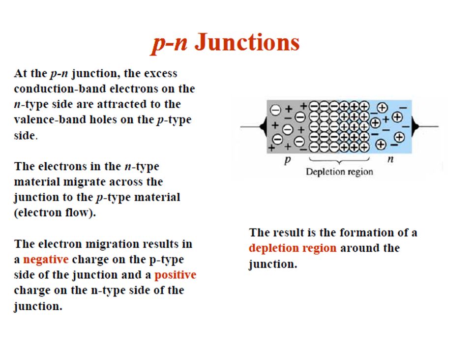
diode : consists of p-type and n-type SC placed in junction with one another. (Si or Ge material)
")
21
Actual Diode Characteristics

25
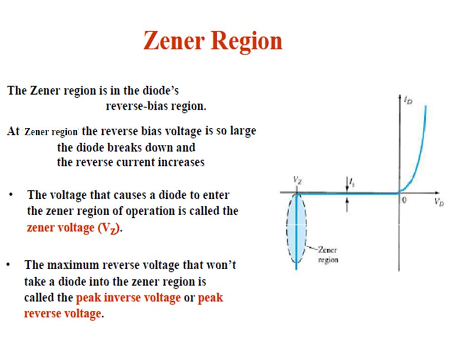
Diode Operating Conditions

26
Diode Operating Conditions

27
Diode Operating Conditions

30
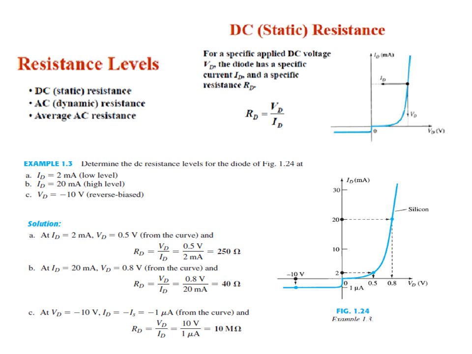
* Found from the graph

37
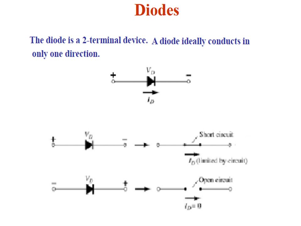
Diodes:

38
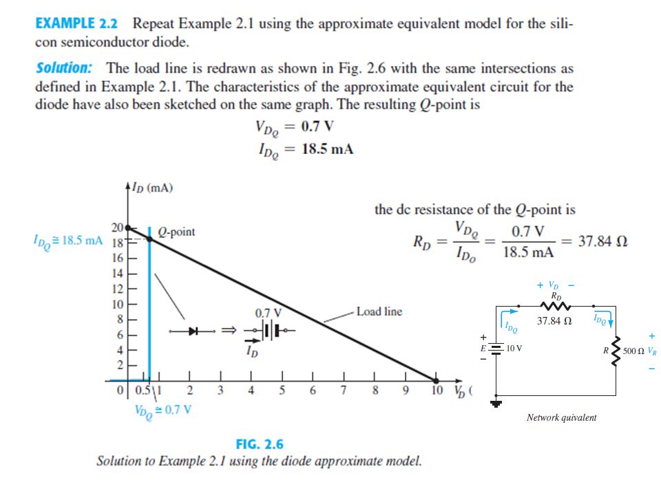
Load-Line Analysis of a Diode
The analysis of diode can follow one of two paths: using the actual characteristics applying an approximate model for the device. Load Line Analysis: used to analyze diode circuit * This circuit will be used to describe the analysis of a diode circuit using its actual characteristics * Later, we will replace the characteristics by an approximate model for the diode and compare solutions

39
Load Line analysis Eq.2.1 Eq.2.2 Eq.2.3.
* The straight line is called the load line because the intersection on the vertical axes is defined by the applied load R. Eq.2.1 Eq.2.2 Eq.2.3. The maximum ID equals E/R , and the maximum VD equals E . The point where the load line and the characteristic curve intersect is the Q-point, which identifies I D and V D for a particular diode in a given circuit.

40
Examples:

41
Solution of Exp.2.1:

42
Solution of Exp.2.1:

Similar presentations


>")

 silicon – Doping – Carrier concentrations.>")
>")


 Also:n 0 p 0 = n.>")


 ©2003 Glencoe/McGraw-Hill Charles A. Schuler.>")


