Download presentation
Presentation is loading. Please wait.

1
Development of radiation hard Sensors & Cables for the CBM Silicon Tracking System Sudeep Chatterji On behalf of CBM-STS Collaboration GSI Helmholtz Centre for Heavy Ion Research 6 th Trento Workshop on Advanced Silicon Radiation Detectors 04 March, 2011

2
3-Dimensional Grid 3-D TCAD simulation tools “SYNOPSYS” Sub packages Sentaurus Inspect Tecplot SPICE (Mixed Mode) Raphael (Used for Kapton simulation)
 Raphael (Used for Kapton simulation)")
3
3-D Grid for orthogonal strips

4
X-Y plane of the 3-D Stereo Angled Grid

5
Simulated Vs. Measured Leakage Current Default Minority Carrier lifetime Modified Minority Carrier life time Electrons = 1e-5 s; Holes = 3e-6 s Electrons = 1e-3 s; Holes = 3e-4s

6
Simulated Vs. Measured Backplane Capacitance

7
Radiation Damage in Silicon University of Perugia Trap Model

8
Comparison with Irradiated Sensors

9
SampleInt. flux (n/cm 2 ) Bias current (at +20) (nA) Measured Bias current (at +20) (nA) Simulated V_ fd (V) Measure d V_ fd (V) Simulated tw_12.06e125.4e35.68e347±545 tw_23.03e129.5e38.31e329±537 tw_83.93e121.07e4 29±532 tw_511.20e123.51e43.03e49±69 tw_320.60e126.65e45.88e431±548 Comparison with Irradiated Sensors Simulated leakage current bit smaller than measured. Due to high value of Minority Carrier life time?
 Bias current (at +20) (nA) Measured Bias current (at +20) (nA) Simulated V_ fd (V) Measure d V_ fd (V) Simulated tw_12.06e125.4e35.68e347±545 tw_23.03e129.5e38.31e329±537 tw_83.93e121.07e4 29±532 tw_511.20e123.51e43.03e49±69 tw_320.60e126.65e45.88e431±548 Comparison with Irradiated Sensors Simulated leakage current bit smaller than measured. Due to high value of Minority Carrier life time .")
10
Comparison with Irradiated Sensors α = (3.99±0.03) x 10 -17 A/cm @ 293K after an annealing of 80 min@600 C Ref: M.Moll, Radiation damage in silicon particle detectors – microscopic defects and Macroscopic properties, Thesis/Dissertation, Hamburg, 1999.
 x K after an annealing of 80 C Ref: M.Moll, Radiation damage in silicon particle detectors – microscopic defects and Macroscopic properties, Thesis/Dissertation, Hamburg, 1999.")
11
Comparison with Irradiated Sensors

12
Exploring Isolation Techniques

13
Breakdown Mechanism in DSSDs Electric Field Distribution on the Ohmic Side

14
Breakdown Mechanism in DSSDs Breakdown occurs in the Coupling Oxide

16
Structure of kapton cable Two connecting layers with constant pitch of 100 μm are laminated together with a lateral shift of 50 μm. A spacer layer is inserted between the two layers to reduce the capacitance. An external shielding layer is applied to reduce the noise. 16

18
Simulation of D0 cable using RAPHAEL 18

19
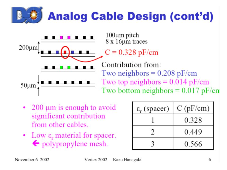
ε r C_total (pF/cm) C int (top)C int (bottom)C int (imm.) 1 0.3280.0140.0170.208 2 0.449--- 3 0.566--- ε r C_total (pF/cm) C int (top)C int (bottom)C int (imm.) 10.460.0190.0170.174 20.580.0260.0240.184 30.690.0320.0280.20 Cables for D0 collaboration By ANSYS By RAPHAEL 19
 C int (top)C int (bottom)C int (imm.) ε r C_total (pF/cm) C int (top)C int (bottom)C int (imm.) Cables for D0 collaboration By ANSYS By RAPHAEL 19")
20
Comparison of CBM, D0 and LHCb kapton cables Parameters CBM cables (new) D0 cables LHCb Cables Trace width 36µm (46µm) 16µm Trace height 14µm 8µm Aspect Ratio 2.6 (3.3) 2 2 Metal traces Aluminum Copper Height of kapton layer 10µm 50µm 100µm Height of spacer 50µm 200µm - Pitch 100µm 112µm Total Capacitance (pF/cm) 0.8 (1.0) 0.5 0.4
 D0 cables LHCb Cables Trace width 36µm (46µm) 16µm Trace height 14µm 8µm Aspect Ratio 2.6 (3.3) 2 2 Metal traces Aluminum Copper Height of kapton layer 10µm 50µm 100µm Height of spacer 50µm 200µm - Pitch 100µm 112µm Total Capacitance (pF/cm) 0.8 (1.0)")
21
Ways to reduce the capacitance of cables Capacitance decreases with decreasing the width of traces Capacitances decreases with increase in height of spacer

22
Effect of trace width on Resistance ENC = 13 * C_tot*

23
ENC versus trace width in kapton cables

24
ENC versus trace height in kapton cables

25
Summary and Future Plans Major contributors to noise are the capacitance and series resistance Detector trace resistance can be ↓ed by ↑ing the thickness of AC pad Detector capacitance will ↑ after irradiation, hence noise will ↑ with irradiation Lesser the width of traces less is the capacitance contributions from cable as trace width contributes more to the capacitance value than the trace height Using Copper can help in reducing cable noise Combination of small sensor + large cables is better than big sensor + small cables Study aspect ratio factor Understand the impact on strip isolation after irradiation and hence on charge collection.

27
Signal to Noise Ratio The most important noise contributions are: 1) Detector Leakage Current (ENC l ) 2) Detector + Cable Capacitance (ENC C ) 3) Detector Parallel Resistor (ENC RP ) 4) Detector + Cable Series Resistor (ENC RS ) The overall noise is the quadratic sum of all contributions:
 Detector Leakage Current (ENC l ) 2) Detector + Cable Capacitance (ENC C ) 3) Detector Parallel Resistor (ENC RP ) 4) Detector + Cable Series Resistor (ENC RS ) The overall noise is the quadratic sum of all contributions:")
28
Noise due to Leakage Current Assuming an amplifier with an integration time (“peaking time”) t p followed by a CR-RC filter the noise contribution by the leakage current can be written as: Using the physical constants, the leakage current in nA and the integration time in µs, the formula can be simplified to: To minimize this noise contribution the detector should be of high quality with small leakage current and the integration time should be short.
 t p followed by a CR-RC filter the noise contribution by the leakage current can be written as: Using the physical constants, the leakage current in nA and the integration time in µs, the formula can be simplified to: To minimize this noise contribution the detector should be of high quality with small leakage current and the integration time should be short.")
29
Noise due to Capacitance The detector + Cable capacity at the input of a charge sensitive amplifier is usually the dominant noise source in the detector system. This noise term can be written as: The parameter a and b are given by the design of the amplifier. C is the total capacitance at the input of the amplifier. Typical values are (amplifier with 1µs integration time): a = 160 e and b = 12 e/pF “a” increases as the electronics become faster.
: a = 160 e and b = 12 e/pF a increases as the electronics become faster..")
30
Noise due to Parallel Resistor The parallel resistor R P in the alternate circuit diagram is the bias resistor. The noise term can be written as: Assuming a temperature of 300 K, t P in µs and R P in MΩ the formula can be simplified to: To achieve low noise, the parallel (bias) resistor should be large! However the value is limited by the production process and the voltage drop across the resistor (high in irradiated detectors).
 resistor should be large. However the value is limited by the production process and the voltage drop across the resistor (high in irradiated detectors)..")
31
Noise due to Series Resistor The series resistor R S in the alternate circuit diagram is given by resistance of connection between strips and amplifier input (e.g. aluminum readout lines, hybrid connections etc.). It can be written as: Note that, in this noise contribution t P is inverse, hence a long t P reduces the noise. The capacitance (from Sensor + Cable) is again responsible for larger noise. To avoid excess noise the aluminum lines should have low resistance (e.g. thick aluminum layer) and all other connections as short as possible.
. It can be written as: Note that, in this noise contribution t P is inverse, hence a long t P reduces the noise. The capacitance (from Sensor + Cable) is again responsible for larger noise. To avoid excess noise the aluminum lines should have low resistance (e.g. thick aluminum layer) and all other connections as short as possible..")
32
Noise dependence on shaping time

33
CBM Tracker: Small sensor +Large Cables (n XYTER slow) ★ readout chip: a = 200 e, b = 13 e/pF, tp = 140 ns ★ 1 detector of 1.5 cm long Strips, C = 6.11 pF and a cable of length 40cm, C = 37.2 pF ➔ ENC_c = 763 e ★ max. leakage current/strip: I ≈ 0.5 nA ➔ ENC_I = 27 e ★ bias resistor Rp = 2 MΩ ➔ ENC_Rp = 204 e ★ series resistor from sensors of 1.5cm long strips = 32 Ω, from cable of length 40cm = 17.5 Ω ➔ ENC_Rs = 322 e ➔ Total noise: ENC = 853 e ENC calculation for CBM tracker

34
CBM Tracker: Small sensor +Large Cables (n XYTER fast) ★ readout chip: a = 200 e, b = 27 e/pF, tp = 19 ns ★ 1 detector of 1.5 cm long Strips, C = 6.11 pF and a cable of length 40cm, C = 37.2 pF ➔ ENC_c = 1369 e ★ max. leakage current/strip: I ≈ 0.5 nA ➔ ENC_I = 10 e ★ bias resistor Rp = 2 MΩ ➔ ENC_Rp = 75 e ★ series resistor from sensors of 1.5cm long strips = 32 Ω, from cable of length 40cm = 17.5 Ω ➔ ENC_Rs = 873 e ➔ Total noise: ENC = 1625 e ENC calculation for CBM tracker

35
CBM Tracker: Big sensor + Small Cables (n XYTER fast) ★ readout chip: a = 200 e, b = 27 e/pF, tp = 19 ns ★ 1 detector of 10 cm long Strips, C = 40.7 pF and a cable of length 10cm, C = 9.3 pF ➔ ENC_c = 1550 e ★ max. leakage current/strip: I ≈ 3.1nA ➔ ENC_I = 26 e ★ bias resistor Rp = 2 MΩ ➔ ENC_Rp = 75 e ★ series resistor from sensors of 10 cm long strips = 213 Ω, from cable of length 10cm = 4.4 Ω ➔ ENC_Rs = 2114 e ➔ Total noise: ENC = 2623 e ENC calculation for CBM tracker

36
CBM Tracker: Big sensor + Small Cables (n XYTER slow) ★ readout chip: a = 200 e, b = 13 e/pF, tp = 140 ns ★ 1 detector of 10 cm long Strips, C = 40.7 pF and a cable of length 10cm, C = 9.3 pF ➔ ENC_c = 850 e ★ max. leakage current/strip: I ≈ 3.1nA ➔ ENC_I = 71 e ★ bias resistor Rp = 2 MΩ ➔ ENC_Rp = 204 e ★ series resistor from sensors of 10 cm long strips = 213 Ω, from cable of length 10cm = 4.4 Ω ➔ ENC_Rs = 779 e ➔ Total noise: ENC = 1173 e ENC calculation for CBM tracker

Similar presentations


>")


 Status of DSSD Sensors.>")


 The SCT requirements: Hermetic lightweight tracker. 4 space-points detection up to pseudo rapidity.>")

1 MeV eq-n cm -2 02.113.6 *10 13 13.55.7*10 13 25.92.3*10 13 39.11.1*10 13 411.90.7*10 13 514.70.5*10.>")
mrad: The Outer Tracker: covers the large.>")
