Download presentation
Presentation is loading. Please wait.

1
High-Performance FPGA-Controlled Amplifier Phase IV May 05-28 April 27 th, 2005

2
Team Information Members: Jimmy Tjoa, EE Agus Leonardo, EE Ian Overton, CprE Client: Teradyne Corporation Faculty Advisor: Dr. Chris Chu May 05-28

3
Outline May 05-28 Resources and Schedules Personnel Effort Other Resources Financial Requirement Schedules Closing Material Project Evaluation Commercialization Additional Work Lessons Learned Risk and Management Closing Summary Introductory Material List of Definitions Acknowledgement Problem Statement & General Solutions Operation Environment Intended Users and Uses Assumptions and Limitations End Product and other Deliverables Project Activity Description Previous Accomplishments Present Accomplishments Approach Considered & Used Definition Activities Design Constraints Research Activities Design Activities Implementation Activities Testing Activities Other Activities

4
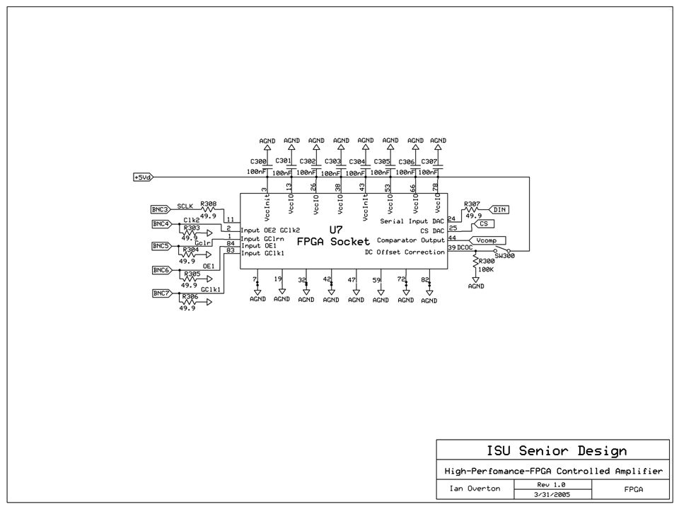
List of Definitions Art-work – Copper layer for Printed Circuit Board (PCB) Bill of Materials – List of Components and their cost DAC – Conversion of a digital signal to an analog sampled signal DC-offset correction – Matched I/O DC-Voltage FPGA – Field programmable gate arrays, allows us to control some the circuits automatically Gain – The ratio of the output amplitude to the input amplitude Input Impedance – the load placed on the circuit driving an input Spectrum Analyzer – A computer-based tool that analyzes signals in the frequency domain Q-Value – The distance between the upper and lower frequency May 05-28
 Bill of Materials – List of Components and their cost DAC – Conversion of a digital signal to an analog sampled signal DC-offset correction – Matched I/O DC-Voltage FPGA – Field programmable gate arrays, allows us to control some the circuits automatically Gain – The ratio of the output amplitude to the input amplitude Input Impedance – the load placed on the circuit driving an input Spectrum Analyzer – A computer-based tool that analyzes signals in the frequency domain Q-Value – The distance between the upper and lower frequency May 05-28")
5
Introduction The purpose: Design a high-performance FPGA-controlled amplifier Teradyne Corporation will use it for a front-end spectrum analyzer The overall goal: Characterize a frequency of up to 100MHz Achieve gain of 6dB, 20dB, 40dB, and 60dB Low Distortion and Noise DC-Offset correction May 05-28

6
Acknowledgement Teradyne Corporation Jacob Mertz Eli Roth Ramon De La Cruz Steven Miller Others Faculty Advisors Dr. Chris Chu Dr. Gary Tuttle Technical Advisors Dr. Randy Geiger Dr. Robert Weber May 05-28

7
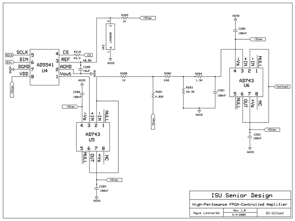
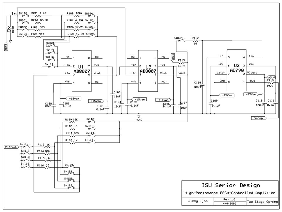
Problem Statement & Solutions DC-Offset Correction Better DAC Fix DC-Voltage Range Amplifier Input Impedance Input impedance changes over gains, so a 50 Ω load was added Increase the Q-Values resistors to make a higher impedance without the load Higher Bandwidth with Lower Distortion and Noise Change Q-Values Ratio Find a better Operational Amplifier Lost a Team Member Larger Work Load Removed Frequency Response Calibration Changed FPGA switching automation to switching manually Loss of a Technical Documentation Research and Verify Previous General Design Write up lost Technical Documentation May 05-28

8
Operating Environment The system should be used in a climate- controlled laboratory at room temperature with low humidity. May 05-28

9
Intended Users and Uses The Teradyne Corporation Engineers Educational purposes May 05-28

10
Assumptions and Limitations The design team assumes that: End product will not be sold DC-offset correction turned on and off manually Gains changed manually The design team’s limitations are: DC-offset voltage kept below ± 1mV Art-work prototype not be accurate as the circuit fabricated Cost must not exceed $3000 Input impedance close to 50 Ω Design requirements meet the design specifications May 05-28

11
Design Specifications DC — 1kHz+/- 5 volts6, 20, 40, 60+/- 10 volts0.05 dB< - 105 dB1.5 nV/rtHz > 1kHz - 20 kHz+/- 5 volts6, 20, 40, 60+/- 10 volts0.05 dB< - 95 dB1.5 nV/rtHz > 20kHz - 100kHz+/- 2.5 volts6, 20, 40+/- 5 volts0.10 dB< -85 dB2.5 nV/rtHz > 100kHz - 1MHz+/- 2.5 volts6, 20, 40+/- 5 volts0.10 dB< - 80 dB3.5 nV/rtHz > 1MHz - 10MHz+/- 2.5 volts6, 20, 40+/- 5 volts0.10 dB< - 70 dB3.5 nV/rtHz > 10MHz - 20MHz+/- 2.5 volts6, 20+/- 5 volts0.10 dB< -65 dB3.5 nV/rtHz > 20MHz - 50MHz+/- 1.0 volts6, 20+/- 2.0 volts0.10 dB< -50 dB5.0 nV/rtHz > 50MHz - 100MHz+/- 1.0 volts6, 20+/- 2.0 volts0.10 dB< -40 dB5.0 nV/rtHz Input Total InputVoltageAvailableMax OutputFreq ResponseHarmonic FrequencyRangeGain SettingsVoltageFlatnessDistortionNoise Range(Volts)(dB)(Volts)(dB) (nV/rtHz) May 05-28
(dB)(Volts)(dB) (nV/rtHz) May 05-28")
12
End Product and Other Deliverables Final product will be used as a front-end spectrum analyzer Deliverables Simulations for Verification Final Schematic Final Art-work Bill of Materials May 05-28

13
Previous Accomplishments FPGA code General Design Operational Amplifier Topology Simulation May 05-28

14
Present Accomplishments Research & Verification Final Schematic Final Art-Work Bill of Materials May 05-28

15
Approach Considered & Used PSpice was chosen over Cadence to simulate and verify the two stage operational amplifier Easy to use PSpice models easy to obtain Art-work was chosen over fabrication for verification Dip switch was chosen over Mechanical Relays due to insufficient time The team evaluated the previous work done on the design and researched if it was the best approach for each subsystem Modifications on art-work and schematic were done using ExpressPCB software Max Plus II will be used to program the FPGA Amplifiers Considered Regular two-stage amplifier Special two-stage amplifier Regular three-stage amplifier May 05-28

16
Special Two-Stage Amplifier May 05-28 http://seniord.ee.iastate.edu/may0528/01084375.pdf

17
Definition Activities Goals of this project: Research & Verify the previous design 100Mhz gains DC-offset correction Fabrication Art-work was chosen Frequency response Removed due to lost a team member Testing Insufficient time May 05-28

18
Design Constraints Parts – High quality, precision parts are required to obtain the specified design requirements for high bandwidth with low noise and distortion Cost – The cost must not exceed $3000 to complete the project DC-offset correction – An appropriate design circuit was assigned Approval – Teradyne must approve the design before the design is implemented May 05-28

19
Research Activities Study previous team’s design Amplifier topology Better Components New resistor values found Removing peaking Input impedance Optimized the DAC May 05-28

20
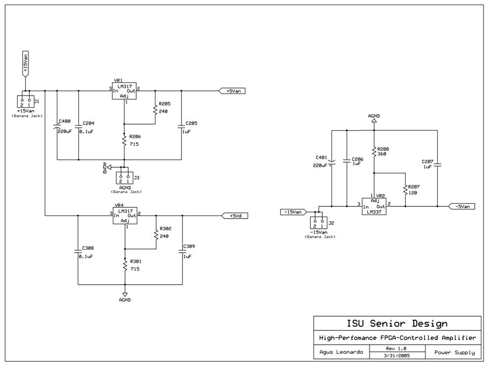
Design Activities Design schematic and art-work for: DC Offset Operational Amplifier FPGA May 05-28

25
Layout

26
Implementation Activities Art-work Schematic Add 50 Ω Input Load Impedance Add Buffer to the output DAC Bill of Materials May 05-28

27
Testing Activities Simulations for operational amplifiers Peaking Input Impedance Bandwidth Simulations for the resistive network in order to get a correct DC voltage range May 05-28

28
Other Activities Weekly report Team meetings Project plan Poster Design report Final report Presentation May 05-28

29
Resources and Schedules May 05-28

30
Other Resource Requirement Item TeamTeam HoursCost Printing of project poster 20$ 71.00 Documentations83$ 20.00 Board120$1343.80 Total223$ 770.40 May 05-28

31
Financial Requirement ItemsW/O Labor With Labor($12/hour) Posters$ 71.00$ 311.00 Board $1343.80 $ 2783.80 Documentations$ 20.00 $ 1016.00 Subtotal $ 1434.80$4110.80 Labor( $12.00 / hour) Jimmy Tjoa$1704.00 Agus Leonardo$2748.00 Ian Overton$2112.00 Subtotal$0.00$ 6564.00 Total $ 1434.80 $ 10674.80 May 05-28
 Posters$ 71.00$ Board $ $ Documentations$ $ Subtotal $ $ Labor( $12.00 / hour) Jimmy Tjoa$ Agus Leonardo$ Ian Overton$ Subtotal$0.00$ Total $ $ May 05-28")
32
Project Schedules May 05-28

33
Deliverable Schedules May 05-28

34
Closure Materials Corrected the DC Offset voltage Changed resistor network Added a buffer Changed original plan Art-work Operational Amplifier Peaking Input Impedance Bandwidth May 05-28

35
Project Evaluation ActivitiesAccomplishment Project DefinitionsFully met Understanding DesignFully met DC-offset CorrectionFully met Part NumberFully met Final DesignFully met Project ReportingFully met TestingNot attempted May 05-28

36
Commercialization Testing Cost: $1343.80 Art-work Total part costs Spare parts Actual board cost $442.38 Recommended street price $600 Market – consumers who need a high- performance FPGA-controlled amplifier May 05-28

37
Additional Work Testing Automation using a FPGA using mechanical relays Frequency response calibration Fabrication May 05-28

38
Lessons Learned Team gained a lot of knowledge working on the design Art-work on ExpressPCB Integrating new parts into PSpice Communication skills with client and faculty advisor Proper documentations Team should not depend on work done by the previous team Prepare for losing a team member May 05-28

39
Risk and Management Lost of a team member Work cooperatively and efficiently Ensure on time delivery Simulations might not match the output from the circuit Topology might be wrong so team did more research May 05-28

40
Closing Summary Team gained many experiences Designing board layout Researching parts Team Work Working for an outside client Keeping up with technology Meeting deadlines May 05-28

41
Questions ??? May 05-28

Similar presentations


 Dr. Aleksander Dogandzic Bruce Fu (EE) Dr.>")


 Kevin.>")
