Download presentation
Presentation is loading. Please wait.

1
NAND Flash Failure Behavior Sponsored By Micron Technology Inc

2
Group Members and Topics Rob Wells Rob Wells Project Introduction Project Introduction System Integration System Integration Jeremy Hamblin Jeremy Hamblin Firmware Design Firmware Design Roger White Roger White NAND DUT Interface NAND DUT Interface NAND Controller & Timing NAND Controller & Timing David Chu David Chu Host GUI Interface & Application Host GUI Interface & Application Conclusions Conclusions

3
Robert Wells Project Introduction System Integration

4
Introduction to NAND Flash What NAND Flash Memory Is What NAND Flash Memory Is NAND Flash Memory Applications NAND Flash Memory Applications What NAND Flash Memory Is Not What NAND Flash Memory Is Not Project Concept Project Concept An Affordable Platform An Affordable Platform Customizable Usage/Programming Patterns Customizable Usage/Programming Patterns Characterization/Analysis of NAND Behavior Characterization/Analysis of NAND Behavior

5
System Integration High Level View High Level View FPGA System FPGA System Block Diagram Interface Block Diagram Interface SOPC Builder Overview SOPC Builder Overview Component Generation Component Generation HAL (Hardware Abstraction Layer) – NIOS II HAL (Hardware Abstraction Layer) – NIOS II HDL (Hardware Description Language) – Quartus II HDL (Hardware Description Language) – Quartus II Quartus II Overview Quartus II Overview Integration of the FPGA system Integration of the FPGA system Controller Development Controller Development NIOS II Overview NIOS II Overview Device Drivers Device Drivers Firmware Firmware Firmware to Controller Integration Firmware to Controller Integration Host PC to Firmware Integration Host PC to Firmware Integration
 – NIOS II HAL (Hardware Abstraction Layer) – NIOS II HDL (Hardware Description Language) – Quartus II HDL (Hardware Description Language) – Quartus II Quartus II Overview Quartus II Overview Integration of the FPGA system Integration of the FPGA system Controller Development Controller Development NIOS II Overview NIOS II Overview Device Drivers Device Drivers Firmware Firmware Firmware to Controller Integration Firmware to Controller Integration Host PC to Firmware Integration Host PC to Firmware Integration")
6
High Level View SOPC Components: NIOS II Processor SDRAM USB On-Chip Memory LCD Display HAL (Hardware Abstraction Layer) C Code API (Application Programming Interface) HDL (Hardware Description Language) Verilog Code NAND Flash Controller Custom Verilog Code (Roger) Firmware Custom C Code (Jeremy) Quartus II NIOS II Application GUI Interface Program the NAND Flash Analyze/Display Results (David) SOPC Builder (System On a Programmable Chip)
 C Code API (Application Programming Interface) HDL (Hardware Description Language) Verilog Code NAND Flash Controller Custom Verilog Code (Roger) Firmware Custom C Code (Jeremy) Quartus II NIOS II Application GUI Interface Program the NAND Flash Analyze/Display Results (David) SOPC Builder (System On a Programmable Chip)")
7
High Level View Application GUI Interface Program the NAND Flash Analyze/Display Results (David) Configure Memory Usage Memory Range Data Pattern Number of Cycles Analyze Performance Will NAND Flash Work Over the Lifespan of a Given Device?
 Configure Memory Usage Memory Range Data Pattern Number of Cycles Analyze Performance Will NAND Flash Work Over the Lifespan of a Given Device")
8
System Integration High Level View High Level View FPGA System FPGA System Block Diagram Interface Block Diagram Interface SOPC Builder Overview SOPC Builder Overview Component Generation Component Generation HAL (Hardware Abstraction Layer) – NIOS II HAL (Hardware Abstraction Layer) – NIOS II HDL (Hardware Description Language) – Quartus II HDL (Hardware Description Language) – Quartus II Quartus II Overview Quartus II Overview Integration of the FPGA system Integration of the FPGA system Controller Development Controller Development NIOS II Overview NIOS II Overview Device Drivers Device Drivers Firmware Firmware Firmware to Controller Integration Firmware to Controller Integration Host PC to Firmware Integration Host PC to Firmware Integration
 – NIOS II HAL (Hardware Abstraction Layer) – NIOS II HDL (Hardware Description Language) – Quartus II HDL (Hardware Description Language) – Quartus II Quartus II Overview Quartus II Overview Integration of the FPGA system Integration of the FPGA system Controller Development Controller Development NIOS II Overview NIOS II Overview Device Drivers Device Drivers Firmware Firmware Firmware to Controller Integration Firmware to Controller Integration Host PC to Firmware Integration Host PC to Firmware Integration")
9
FPGA development system NAND Flash Controller (Roger) SOPC Built System (Jeremy) Reset Delay Clock Generation
 SOPC Built System (Jeremy) Reset Delay Clock Generation")
10
System Integration High Level View High Level View FPGA System FPGA System Block Diagram Interface Block Diagram Interface SOPC Builder Overview SOPC Builder Overview Component Generation Component Generation HAL (Hardware Abstraction Layer) – NIOS II HAL (Hardware Abstraction Layer) – NIOS II HDL (Hardware Description Language) – Quartus II HDL (Hardware Description Language) – Quartus II Quartus II Overview Quartus II Overview Integration of the FPGA system Integration of the FPGA system Controller Development Controller Development NIOS II Overview NIOS II Overview Device Drivers Device Drivers Firmware Firmware Firmware to Controller Integration Firmware to Controller Integration Host PC to Firmware Integration Host PC to Firmware Integration
 – NIOS II HAL (Hardware Abstraction Layer) – NIOS II HDL (Hardware Description Language) – Quartus II HDL (Hardware Description Language) – Quartus II Quartus II Overview Quartus II Overview Integration of the FPGA system Integration of the FPGA system Controller Development Controller Development NIOS II Overview NIOS II Overview Device Drivers Device Drivers Firmware Firmware Firmware to Controller Integration Firmware to Controller Integration Host PC to Firmware Integration Host PC to Firmware Integration")
11
Example FPGA System With SOPC

12
System Integration High Level View High Level View FPGA System FPGA System Block Diagram Interface Block Diagram Interface SOPC Builder Overview SOPC Builder Overview Component Generation Component Generation HAL (Hardware Abstraction Layer) – NIOS II HAL (Hardware Abstraction Layer) – NIOS II HDL (Hardware Description Language) – Quartus II HDL (Hardware Description Language) – Quartus II Quartus II Overview Quartus II Overview Integration of the FPGA system Integration of the FPGA system Controller Development Controller Development NIOS II Overview NIOS II Overview Device Drivers Device Drivers Firmware Firmware Firmware to Controller Integration Firmware to Controller Integration Host PC to Firmware Integration Host PC to Firmware Integration
 – NIOS II HAL (Hardware Abstraction Layer) – NIOS II HDL (Hardware Description Language) – Quartus II HDL (Hardware Description Language) – Quartus II Quartus II Overview Quartus II Overview Integration of the FPGA system Integration of the FPGA system Controller Development Controller Development NIOS II Overview NIOS II Overview Device Drivers Device Drivers Firmware Firmware Firmware to Controller Integration Firmware to Controller Integration Host PC to Firmware Integration Host PC to Firmware Integration")
14
System Integration High Level View High Level View FPGA System FPGA System Block Diagram Interface Block Diagram Interface SOPC Builder Overview SOPC Builder Overview Component Generation Component Generation HAL (Hardware Abstraction Layer) – NIOS II HAL (Hardware Abstraction Layer) – NIOS II HDL (Hardware Description Language) – Quartus II HDL (Hardware Description Language) – Quartus II Quartus II Overview Quartus II Overview Integration of the FPGA system Integration of the FPGA system Controller Development Controller Development NIOS II Overview NIOS II Overview Device Drivers Device Drivers Firmware Firmware Firmware to Controller Integration Firmware to Controller Integration Host PC to Firmware Integration Host PC to Firmware Integration
 – NIOS II HAL (Hardware Abstraction Layer) – NIOS II HDL (Hardware Description Language) – Quartus II HDL (Hardware Description Language) – Quartus II Quartus II Overview Quartus II Overview Integration of the FPGA system Integration of the FPGA system Controller Development Controller Development NIOS II Overview NIOS II Overview Device Drivers Device Drivers Firmware Firmware Firmware to Controller Integration Firmware to Controller Integration Host PC to Firmware Integration Host PC to Firmware Integration")
16
System Integration High Level View High Level View FPGA System FPGA System Block Diagram Interface Block Diagram Interface SOPC Builder Overview SOPC Builder Overview Component Generation Component Generation HAL (Hardware Abstraction Layer) – NIOS II HAL (Hardware Abstraction Layer) – NIOS II HDL (Hardware Description Language) – Quartus II HDL (Hardware Description Language) – Quartus II Quartus II Overview Quartus II Overview Integration of the FPGA system Integration of the FPGA system Controller Development Controller Development NIOS II Overview NIOS II Overview Device Drivers Device Drivers Firmware Firmware Firmware to Controller Integration Firmware to Controller Integration Host PC to Firmware Integration Host PC to Firmware Integration
 – NIOS II HAL (Hardware Abstraction Layer) – NIOS II HDL (Hardware Description Language) – Quartus II HDL (Hardware Description Language) – Quartus II Quartus II Overview Quartus II Overview Integration of the FPGA system Integration of the FPGA system Controller Development Controller Development NIOS II Overview NIOS II Overview Device Drivers Device Drivers Firmware Firmware Firmware to Controller Integration Firmware to Controller Integration Host PC to Firmware Integration Host PC to Firmware Integration")
17
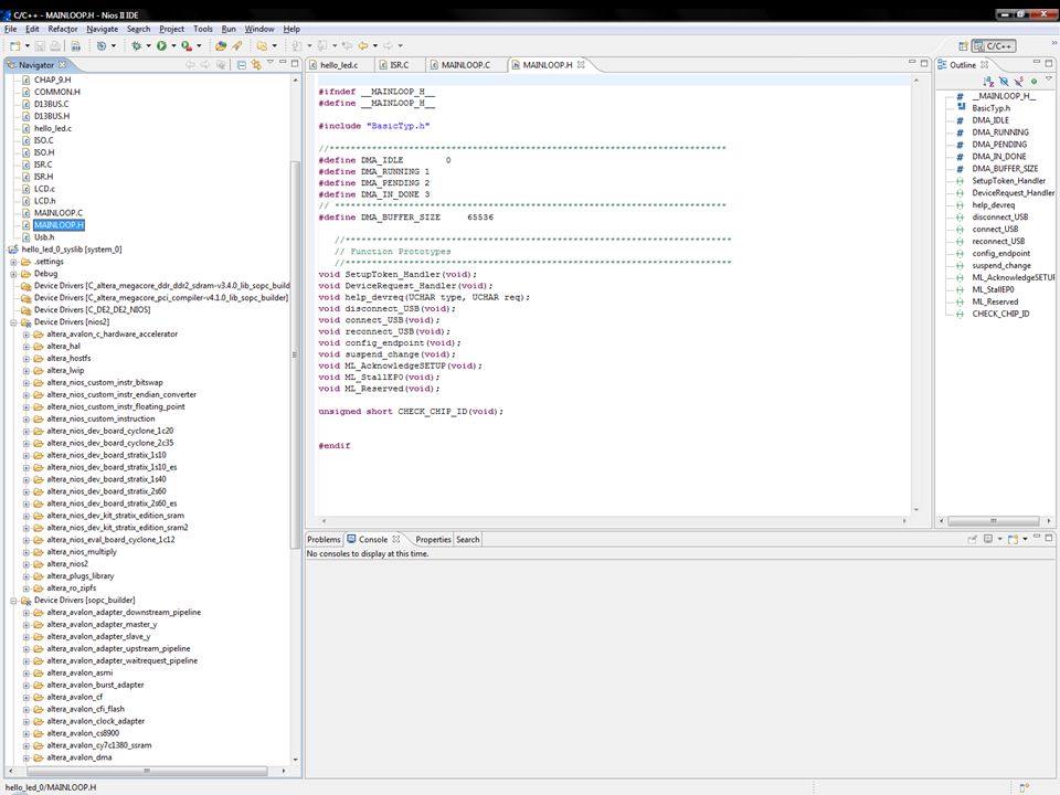
Firmware to Controller Integration Firmware C Code NIOS II Controller Verilog Quartus II Buffer SOPC Builder

18
System Integration High Level View High Level View FPGA System FPGA System Block Diagram Interface Block Diagram Interface SOPC Builder Overview SOPC Builder Overview Component Generation Component Generation HAL (Hardware Abstraction Layer) – NIOS II HAL (Hardware Abstraction Layer) – NIOS II HDL (Hardware Description Language) – Quartus II HDL (Hardware Description Language) – Quartus II Quartus II Overview Quartus II Overview Integration of the FPGA system Integration of the FPGA system Controller Development Controller Development NIOS II Overview NIOS II Overview Device Drivers Device Drivers Firmware Firmware Firmware to Controller Integration Firmware to Controller Integration Host PC to Firmware Integration Host PC to Firmware Integration
 – NIOS II HAL (Hardware Abstraction Layer) – NIOS II HDL (Hardware Description Language) – Quartus II HDL (Hardware Description Language) – Quartus II Quartus II Overview Quartus II Overview Integration of the FPGA system Integration of the FPGA system Controller Development Controller Development NIOS II Overview NIOS II Overview Device Drivers Device Drivers Firmware Firmware Firmware to Controller Integration Firmware to Controller Integration Host PC to Firmware Integration Host PC to Firmware Integration")
19
Host PC to Firmware Integration Phillips ISP1362 (USB) SOPC Builder (HAL) NIOS II (Device Driver) WinDriver (Device Driver)
 SOPC Builder (HAL) NIOS II (Device Driver) WinDriver (Device Driver)")
20
Conclusions System Components System Components Custom Hardware Design (Verilog) Custom Hardware Design (Verilog) Custom Firmware Design (C) Custom Firmware Design (C) Powerful Design Tools Powerful Design Tools Custom Built Application GUI Interface Custom Built Application GUI Interface Inexpensive Platform for Testing Inexpensive Platform for Testing Analysis of NAND Wear-Out From a Customizable Memory Usage Model Analysis of NAND Wear-Out From a Customizable Memory Usage Model Allows Developers to Determine if NAND Flash is a Viable Solution for a Given Application Allows Developers to Determine if NAND Flash is a Viable Solution for a Given Application Evaluate Other Aspects of NAND Flash Evaluate Other Aspects of NAND Flash
 Custom Hardware Design (Verilog) Custom Firmware Design (C) Custom Firmware Design (C) Powerful Design Tools Powerful Design Tools Custom Built Application GUI Interface Custom Built Application GUI Interface Inexpensive Platform for Testing Inexpensive Platform for Testing Analysis of NAND Wear-Out From a Customizable Memory Usage Model Analysis of NAND Wear-Out From a Customizable Memory Usage Model Allows Developers to Determine if NAND Flash is a Viable Solution for a Given Application Allows Developers to Determine if NAND Flash is a Viable Solution for a Given Application Evaluate Other Aspects of NAND Flash Evaluate Other Aspects of NAND Flash")
21
Questions

22
Jeremy Hamblin Firmware Design

23
SOPC Builder SOPC Builder System Components System Components Firmware Design (NIOS II) Firmware Design (NIOS II) Reset NAND Operation Reset NAND Operation USB Interface USB Interface Op-Code/Algorithm Op-Code/Algorithm NAND Flash Addressing NAND Flash Addressing Example Algorithm Layout Example Algorithm Layout Command Transferring Command Transferring
 Firmware Design (NIOS II) Reset NAND Operation Reset NAND Operation USB Interface USB Interface Op-Code/Algorithm Op-Code/Algorithm NAND Flash Addressing NAND Flash Addressing Example Algorithm Layout Example Algorithm Layout Command Transferring Command Transferring")
24
SOPC Builder (System On a Programmable Chip) NIOS II Processor SDRAM Instruction & Data Block Mapping & Status Displays Global Reset USB Buffer Read Enable
 NIOS II Processor SDRAM Instruction & Data Block Mapping & Status Displays Global Reset USB Buffer Read Enable")
25
Firmware Design SOPC Builder SOPC Builder System Components System Components Firmware Design (NIOS II) Firmware Design (NIOS II) Reset NAND Operation Reset NAND Operation USB Interface USB Interface Op-Code/Algorithm Op-Code/Algorithm NAND Flash Addressing NAND Flash Addressing Example Algorithm Layout Example Algorithm Layout Command Transferring Command Transferring
 Firmware Design (NIOS II) Reset NAND Operation Reset NAND Operation USB Interface USB Interface Op-Code/Algorithm Op-Code/Algorithm NAND Flash Addressing NAND Flash Addressing Example Algorithm Layout Example Algorithm Layout Command Transferring Command Transferring")
26
Firmware Design Reset NAND Operation Reset NAND Operation First Operation After NAND Power Up First Operation After NAND Power Up Occurs During System Initialization Occurs During System Initialization Places NAND DUT (Device Under Test) in a Known State Places NAND DUT (Device Under Test) in a Known State
 in a Known State Places NAND DUT (Device Under Test) in a Known State")
27
Firmware Design SOPC Builder SOPC Builder System Components System Components Firmware Design (NIOS II) Firmware Design (NIOS II) Reset NAND Operation Reset NAND Operation USB Interface USB Interface Op-Code/Algorithm Op-Code/Algorithm NAND Flash Addressing NAND Flash Addressing Example Algorithm Layout Example Algorithm Layout Command Transferring Command Transferring
 Firmware Design (NIOS II) Reset NAND Operation Reset NAND Operation USB Interface USB Interface Op-Code/Algorithm Op-Code/Algorithm NAND Flash Addressing NAND Flash Addressing Example Algorithm Layout Example Algorithm Layout Command Transferring Command Transferring")
28
Firmware Design USB Interface USB Interface Generates IRQ (Interrupt ReQuest) Generates IRQ (Interrupt ReQuest) ISR (Interrupt Service Routine) Receives Data Sent From Host PC and Parses Data ISR (Interrupt Service Routine) Receives Data Sent From Host PC and Parses Data 00 00 00 00 | 00 00 00 00 | 00 00 00 00 | 00 00 00 00 - 16 Bytes 00 00 00 00 - Byte0 Padding Algorithm OP Code 00 00 00 00 | 00 00 00 00 | 00 00 00 00 | 00 00 00 00 - 16 Bytes Start Address – 3 Bytes End Address – 3 Bytes Padding – 1 Byte 00 00 00 00 | 00 00 00 00 | 00 00 00 00 | 00 00 00 00 - 16 Bytes # Cycles – 3 Bytes Padding – 5 Bytes
 Generates IRQ (Interrupt ReQuest) ISR (Interrupt Service Routine) Receives Data Sent From Host PC and Parses Data ISR (Interrupt Service Routine) Receives Data Sent From Host PC and Parses Data | | | Bytes Byte0 Padding Algorithm OP Code | | | Bytes Start Address – 3 Bytes End Address – 3 Bytes Padding – 1 Byte | | | Bytes # Cycles – 3 Bytes Padding – 5 Bytes")
29
Firmware Design Op-Code Types Op-Code Types Read ID Read ID Write Write Read Read Algorithm Types Algorithm Types Continuous Continuous Checker Board Checker Board Random Random

30
Firmware Design NAND Flash Addressing NAND Flash Addressing Blocks Bytes Pages

31
Firmware Design NAND Flash Addressing NAND Flash Addressing

32
Algorithm Example Continuous Cycle ICycle II Checker Board Block-0 Block-1 … Block N-1 Block N Page N Page N-1 … Page 1Page 0 Erased Programmed

33
Firmware Design SOPC Builder SOPC Builder System Components System Components Firmware Design (NIOS II) Firmware Design (NIOS II) Reset NAND Operation Reset NAND Operation USB Interface USB Interface Op-Code/Algorithm Op-Code/Algorithm NAND Flash Addressing NAND Flash Addressing Example Algorithm Layout Example Algorithm Layout Command Transferring Command Transferring
 Firmware Design (NIOS II) Reset NAND Operation Reset NAND Operation USB Interface USB Interface Op-Code/Algorithm Op-Code/Algorithm NAND Flash Addressing NAND Flash Addressing Example Algorithm Layout Example Algorithm Layout Command Transferring Command Transferring")
34
Firmware Design Command Transferring Command Transferring Commands & Data Transferred Through Buffer Commands & Data Transferred Through Buffer Different Data and Command Requirements Different Data and Command Requirements Write- 2119 Bytes Transferred to NAND, 0 Returned Write- 2119 Bytes Transferred to NAND, 0 Returned Read- 7 Bytes Transferred to NAND, 2112 Returned Read- 7 Bytes Transferred to NAND, 2112 Returned Erase- 5 Bytes Transferred to NAND, 0 Returned Erase- 5 Bytes Transferred to NAND, 0 Returned Read Status- 1 Byte Transferred, 1 Returned Read Status- 1 Byte Transferred, 1 Returned Each NAND Command Type Has its Own Buffer Function Each NAND Command Type Has its Own Buffer Function Removes All NAND Device Timing Constraints From the Firmware Removes All NAND Device Timing Constraints From the Firmware Firmware Too Slow Firmware Too Slow

35
Firmware Design Conclusion Command Received Over USB Command Received Over USB Parsed in USB ISR Parsed in USB ISR Execution of Op-Code Execution of Op-Code Command and Data are Passed to NAND Controller Through the Buffer Command and Data are Passed to NAND Controller Through the Buffer Command is Executed From Start Address to End Address Command is Executed From Start Address to End Address Repeated for # of Cycles Given in Command From Host Repeated for # of Cycles Given in Command From Host Block Status Returned Over USB Block Status Returned Over USB

36
Questions

37
Roger White NAND DUT Interface NAND Controller & Timing

38
NAND DUT Interface Daughter Card Daughter Card Our Own?? Our Own?? Boise State’s Boise State’s

39
NAND DUT Interface

40
NAND Controller & Timing Pins to NAND Chip Pins to NAND Chip Operations Operations

41
NAND Controller & Timing Pins to NAND chip Pins to NAND chip CLE (Command Line Enable) CLE (Command Line Enable) CE# (Chip Enable) CE# (Chip Enable) WE# (Write Enable) WE# (Write Enable) ALE (Address Line Enable) ALE (Address Line Enable) R/B (Ready/Busy) R/B (Ready/Busy) RE# (Read Enable) RE# (Read Enable) WP# (Write Protect) WP# (Write Protect) I/Ox (Input/Output) I/Ox (Input/Output)
 CLE (Command Line Enable) CE# (Chip Enable) CE# (Chip Enable) WE# (Write Enable) WE# (Write Enable) ALE (Address Line Enable) ALE (Address Line Enable) R/B (Ready/Busy) R/B (Ready/Busy) RE# (Read Enable) RE# (Read Enable) WP# (Write Protect) WP# (Write Protect) I/Ox (Input/Output) I/Ox (Input/Output)")
42
NAND Controller & Timing Pins to NAND Chip Pins to NAND Chip Operations Operations

43
NAND Controller & Timing Operations Operations Read Read Program Program Erase Erase Read Status Read Status Reset Reset Read ID Read ID

44
Program Operation Program Operation NAND Controller & timing

45
NAND Controller & Timing Erase Operation Erase Operation

46
NAND Controller & Timing Reset Operation Reset Operation

47
Conclusions NAND DUT Interface Daughter Card NAND Controller & Timing Pins Operations

48
Questions?

49
User Interface, USB, and Conclusions By: David Chu

50
Overview User Interface User Interface Command Interface Command Interface Functionality and Scripting Information Functionality and Scripting Information Results Interface Results Interface Functionality, Database Information, and XML File Description Functionality, Database Information, and XML File Description Charts Interface Charts Interface Functionality Functionality USB USB Functionality and Bit Organization Functionality and Bit Organization Conclusions Conclusions Methods, Results, and Future Improvements Methods, Results, and Future Improvements

51
Three Parts to the UI Command Interface - Allows the user to specify the method and method parameters that are sent to the controller. Command Interface - Allows the user to specify the method and method parameters that are sent to the controller. Results Interface - Allows the user to view, store, load, and search through the results stored in a database Results Interface - Allows the user to view, store, load, and search through the results stored in a database Charts Interface - Allows the viewer to visually see the results in graphical form Charts Interface - Allows the viewer to visually see the results in graphical form

52
Command Interface

54
Command Interface Functionality Allows the user to easily construct commands and send them to the controller Allows the user to easily construct commands and send them to the controller Allows the user to load in scripts to automate the controller Allows the user to load in scripts to automate the controller Allows the user to link to the Results Interface Allows the user to link to the Results Interface

55
Script Files Allow the user to automate the NAND Flash test application through a comma delimited file. Allow the user to automate the NAND Flash test application through a comma delimited file. Script files are written in the following manner: Script files are written in the following manner: Read,000000000101111001000000,000000000110000111000000,Full,200

56
Results Interface

57
Results Interface Functionality Allows the user to easily visualize data that is stored in the database. Allows the user to easily visualize data that is stored in the database. Allows the user to sort items in the table by columns Allows the user to sort items in the table by columns Allows the user to search the data for specific results or a range of results Allows the user to search the data for specific results or a range of results Allows the user to load or save database information into or from an XML file Allows the user to load or save database information into or from an XML file Allows the user to link to the Charts Interface Allows the user to link to the Charts Interface

58
Database Information Uses SQL and runs on Microsoft SQL Server 2005 Uses SQL and runs on Microsoft SQL Server 2005 Contains one table with the following elements: ID, Cycle, MemoryAddress, FunctionName, Status, and Algorithm Contains one table with the following elements: ID, Cycle, MemoryAddress, FunctionName, Status, and Algorithm Contains the following stored procedures: FindID, RemoveID, RemoveAll, InsertID, and UpdateID Contains the following stored procedures: FindID, RemoveID, RemoveAll, InsertID, and UpdateID

59
XML Files - - 1 1 1 6 Write Bad Checker 1 6 Write Bad Checker - - 2 2 15 4 Write Bad Checker 15 4 Write Bad Checker - - Generated from database when the user selects the save button Generated from database when the user selects the save button Allows the user to manipulate the results to their specific needs Allows the user to manipulate the results to their specific needs Allows the user to import data into other applications that support XML Allows the user to import data into other applications that support XML

60
Charts Interface

61
Chart Interface Functionality Allows the user to visually represent the total number of failures over cycles Allows the user to visually represent the total number of failures over cycles Allows the user to turn on and off horizontal and vertical grids Allows the user to turn on and off horizontal and vertical grids

62
Overview User Interface User Interface Command Interface Command Interface Functionality and Scripting Information Functionality and Scripting Information Results Interface Results Interface Functionality, Database Information, and XML File Description Functionality, Database Information, and XML File Description Charts Interface Charts Interface Functionality Functionality USB USB Functionality and Bit Organization Functionality and Bit Organization Conclusions Conclusions Methods, Results, and Future Improvements Methods, Results, and Future Improvements

63
USB Information Connection: USB 2.0 connection Connection: USB 2.0 connection Transfer Rate: USB Full-Speed Transfer Rate (12 Mbps) Transfer Rate: USB Full-Speed Transfer Rate (12 Mbps) Transfer Method: USB Interrupt Transfers Transfer Method: USB Interrupt Transfers PnP Compatible PnP Compatible
 Transfer Rate: USB Full-Speed Transfer Rate (12 Mbps) Transfer Method: USB Interrupt Transfers Transfer Method: USB Interrupt Transfers PnP Compatible PnP Compatible")
64
Bit Organization USB Interface USB Interface Sends 16-Bytes Sends 16-Bytes Bytes are Transferred Using Big Endian Bytes are Transferred Using Big Endian 00 00 00 00 | 00 00 00 00 | 00 00 00 00 | 00 00 00 00 - 16 Bytes 00 00 00 00 - Byte0 Padding Algorithm OP Code 00 00 00 00 | 00 00 00 00 | 00 00 00 00 | 00 00 00 00 - 16 Bytes Start Address – 3 Bytes End Address – 3 Bytes Padding – 1 Byte 00 00 00 00 | 00 00 00 00 | 00 00 00 00 | 00 00 00 00 - 16 Bytes # Cycles – 3 Bytes Padding – 5 Bytes

65
Overview User Interface User Interface Command Interface Command Interface Functionality and Scripting Information Functionality and Scripting Information Results Interface Results Interface Functionality, Database Information, and XML File Description Functionality, Database Information, and XML File Description Charts Interface Charts Interface Functionality Functionality USB USB Functionality and Bit Organization Functionality and Bit Organization Conclusions Conclusions Methods, Results, and Future Improvements Methods, Results, and Future Improvements

66
Project Synopsis Method – used the Altera DE2 development board to create a system consisting of a memory module, a processor, and an FPGA controller in order to enable communication between a host PC test application and NAND Flash. Method – used the Altera DE2 development board to create a system consisting of a memory module, a processor, and an FPGA controller in order to enable communication between a host PC test application and NAND Flash. FPGA/Processor Dev System Host PC USB ver 2.0 Simple GUI DUT

67
Project Synopsis Cont. Results – created an affordable and easy to use application that allows developers to run multiple tests on NAND Flash and easily visualize the results through tabular and graphical methods Results – created an affordable and easy to use application that allows developers to run multiple tests on NAND Flash and easily visualize the results through tabular and graphical methods

68
Future Improvements Redesign the GUI to work with multiple operating systems Redesign the GUI to work with multiple operating systems Configure the NAND Flash controller to operate with NAND Flash from other manufacturers Configure the NAND Flash controller to operate with NAND Flash from other manufacturers Use caching methods to improve the performance of the NAND Flash test application Use caching methods to improve the performance of the NAND Flash test application

69
Questions

70
Thank You: Ken Stevens Ken Stevens Dennis Zattiero Dennis Zattiero Dean Klein Dean Klein Ken Koenig Ken Koenig

Similar presentations


 By Michael Tomer, Cory Shirts, SzeHsiang Harper, Jake Johns.>")


 The Laboratory of Computer Communication and Networking Network Host Analyzer.>")


