Download presentation
Presentation is loading. Please wait.

1
ELECTRONICS II VLSI DESIGN FALL 2013 LECTURE 4 INSTRUCTOR: L.M. HEAD, PhD ELECTRICAL & COMPUTER ENGINEERING ROWAN UNIVERSITY

2
MOSFET Symbols

3
Cross-section used to identify capacitances.

4
Accumulation

5
Depletion – no channel poly SiO 2 P-type substrate GND V << V th Depletion region

6
Depletion – sub threshold channel

7
Inversion

8
Capacitance to ground

9
MOSFET Capacitance Model

10
Threshold Voltage

11
Calculating the Threshold Voltage 1. Develop the depletion region 2. Create a channel at the gate oxide/substrate interface 3. Account for any source to body voltage 4. Neutralize defect charge 5. Neutralize material dependent potential difference Begin with the definition of voltage due to a charge stored on a capacitor. +Q b ’ is the charge on the gate and -Q b ’ is the charge under the gate oxide.

12
Calculating the Threshold Voltage From these equations: If the surface potential, V s is equal to the electrostatic potential in the semiconductor bulk there is no charge stored in a depletion region. As V s increases, the depletion region grows. First, we determine the charge in the depletion region.

13
Next, we determine the additional charge due to the channel. V s increases with an increase in V GS. When V S reaches -V fp negative charge has accumulated at the oxide semiconductor interface. In fact, at that point the interface area (channel) is as n-type as the bulk semiconductor is p-type. Taking into consideration any source to body potential: If the body of the MOSFET is not tied to the source, the potential between the interface and the bulk is not only dependent upon V GS. Now the charge under the gate totals,
 is as n-type as the bulk semiconductor is p-type. Taking into consideration any source to body potential: If the body of the MOSFET is not tied to the source, the potential between the interface and the bulk is not only dependent upon V GS. Now the charge under the gate totals,.")
14
The total potential across the gate-oxide capacitance: Since the change in voltage to obtain the channel is: Then*, *Remember, V fp is a negative number! An additional source of charge is defects at the oxide interface:

15
And finally, there is the inherent potential difference between the gate and the substrate:

16
Combining these components to get the final version of the threshold voltage: Note error in equation 6.17

17
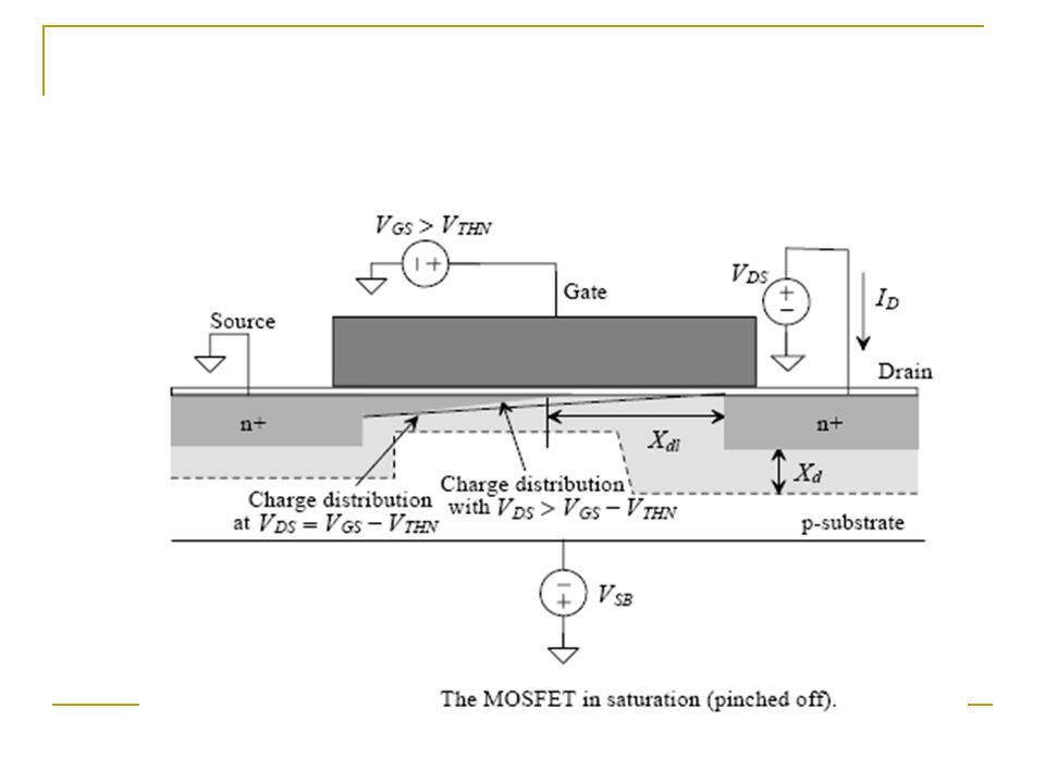
Now we come to the I-V Characteristics

Similar presentations
 Field-Effect Transistors (FET) MOSFET Introduction 1.>")


>")
>")
![EE415 VLSI Design The Devices: MOS Transistor [Adapted from Rabaey’s Digital Integrated Circuits, ©2002, J. Rabaey et al.]](/16/5062541/big_thumb.jpg "EE415 VLSI Design The Devices: MOS Transistor [Adapted from Rabaey’s Digital Integrated Circuits, ©2002, J. Rabaey et al.]>")

 lecture02 Sherief Reda Division of Engineering, Brown University Spring 2008 [sources: Weste/Addison.>")


 – Effect of channel-to-body bias – Small-signal capacitance.>")

