Download presentation
Presentation is loading. Please wait.

1
EEE527 Embedded Systems Lecture 10B:Chapter 11 Analogue to Digital Convertors (ADCs) (version 2: 25/11/13, see after slide 20 Ian McCrumRoom 5B18, Tel: 90 366364 voice mail on 6 th ring Email: IJ.McCrum@Ulster.ac.uk Web site: http://www.eej.ulst.ac.ukIJ.McCrum@Ulster.ac.ukhttp://www.eej.ulst.ac.uk "Adapted from the text “Programming 32-bit Microcontrollers in C – Exploring the PIC32, © 2008.” Lucio di Jasio www.eej.ulster.ac.uk/~ian/modules/EEE527/files
 (version 2: 25/11/13, see after slide 20 Ian McCrumRoom 5B18, Tel: voice mail on 6 th ring Web site: Adapted from the text Programming 32-bit Microcontrollers in C – Exploring the PIC32, © Lucio di Jasio")
2
The DP32 board has AN9 wired to a Variable Resistor AN9 is RB15/RPB15, pin 26 on the 28 pin device

7
The DP32 board has AN9 wired to a Variable Resistor AN9 is RB15/RPB15, pin 26 on the 28 pin device Redo this code for AN9

9
The DP32 board has AN9 wired to a Variable Resistor AN9 is RB15/RPB15, pin 26 on the 28 pin device Redo this code for AN9

11
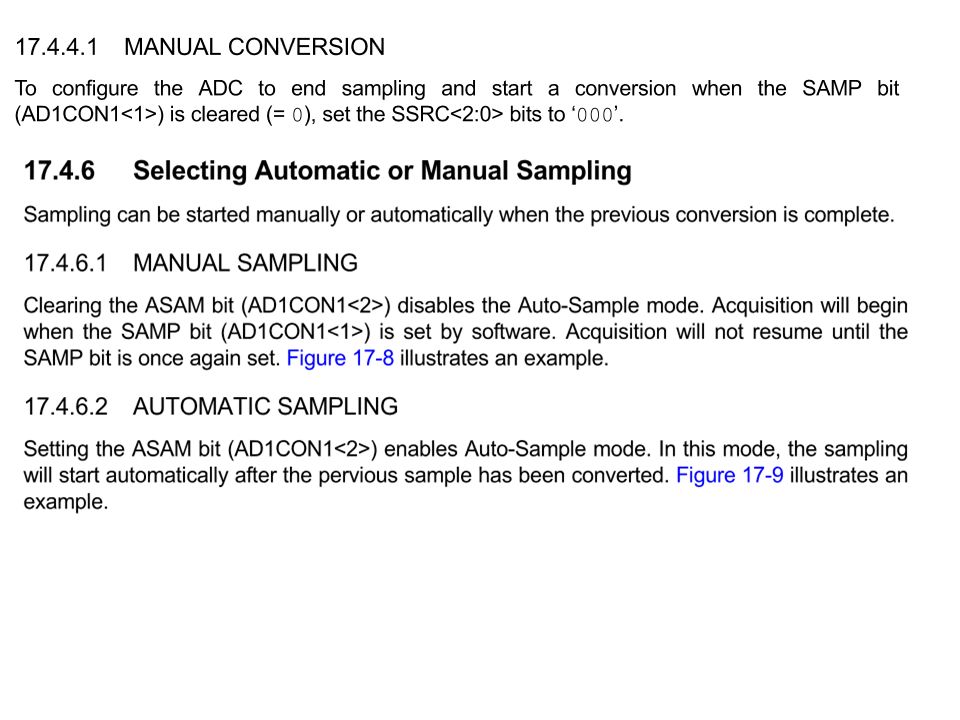
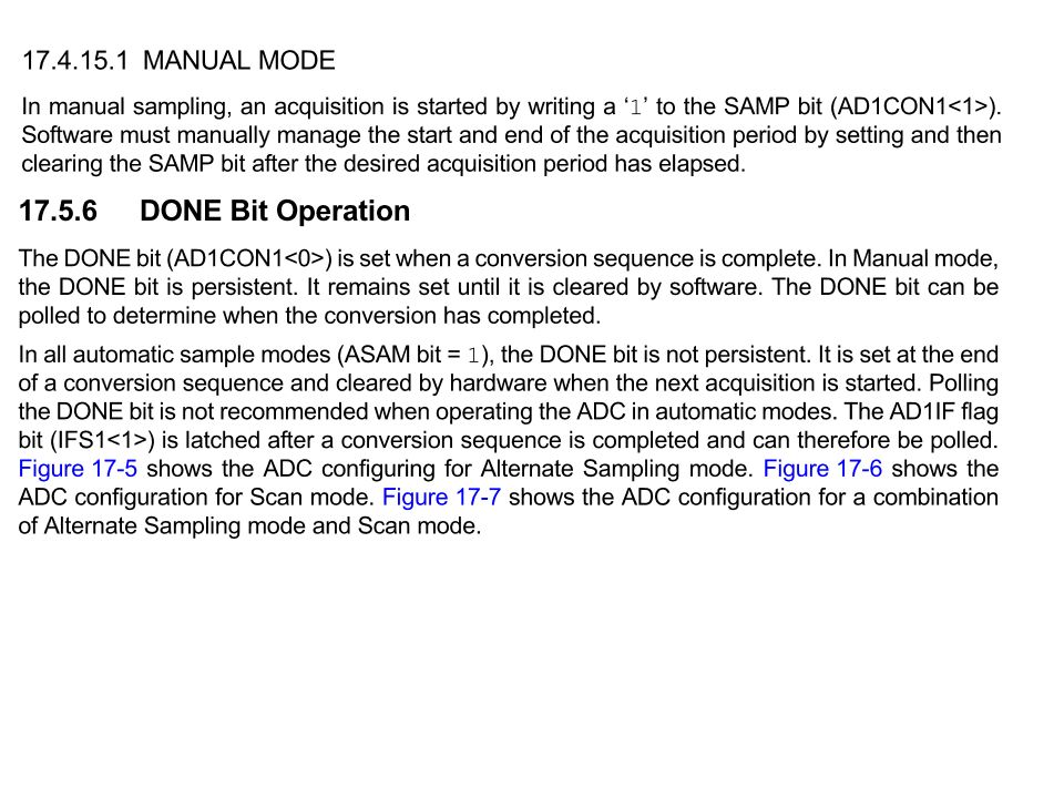
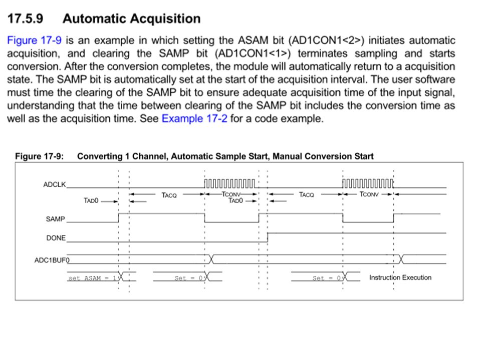
Bit 15 ON 1 = ADC is operating Bit 13 SIDL only relevant in idle mode Bit 10-8 FORM 000 = 16 bit Data out – bottom 10 bits are the reading Bit 7-5 SSRC 000 = clearing SAMP bit ends sampling and starts conversion Bit 4 CLRASAM 0 = normal, buffer get overwritten by next conversion sequence Bit 2 ASAM 1 = sampling begins as soon as last conversion complete 0 = Sampling begins when SAMP bit is set Bit 1 SAMP 1 = ADC sample and hold Amp is sampling 0 = ADC sample and hold Amp is holding When ASAM = 0, writing ‘1’ to this bit starts sampling When SSRC = 000, put ‘0’ in SAMP -ends sampling & starts conversion Bit 0 DONE 1 = ADC conversion is done

12
Bit 15-13 VCFG 000 = Vrefh = AVDD and Vrefl = Avss (3.3V and 0V) Bit 12 OFFCAL 0 = disable input offset calibration Bit 10 CSNA 0 = do not scan inputs {1 = scan inputs} Bit 7 BUFS only valid if BUFM is ‘1’; 1 = ADC is filling buffer 8-F, you read 0-7 0 = ADC is filling buffer 0-7, you read 8-F Bit 5-2 SMPI 0000 = Interrupt at completion of conversion for each sample Bit 1 BUFM 0 = Buffer configures as one 16 word buffer ADC1BUFF to ADC1BUF0 1 = Buffer configures as two 8 word buffers Bit 0 ALTS 0 = Use Sample A input multiplexor settings {1=>alternate sample A/B)
 Bit 12 OFFCAL 0 = disable input offset calibration Bit 10 CSNA 0 = do not scan inputs {1 = scan inputs} Bit 7 BUFS only valid if BUFM is ‘1’; 1 = ADC is filling buffer 8-F, you read = ADC is filling buffer 0-7, you read 8-F Bit 5-2 SMPI 0000 = Interrupt at completion of conversion for each sample Bit 1 BUFM 0 = Buffer configures as one 16 word buffer ADC1BUFF to ADC1BUF0 1 = Buffer configures as two 8 word buffers Bit 0 ALTS 0 = Use Sample A input multiplexor settings {1=>alternate sample A/B)")
13
bit 15 ADRC: ADC Conversion Clock Source bit 1 = Clock derived from FRC 0 = Clock derived from Peripheral Bus Clock (PBCLK) bit 12-8 SAMC : Auto-Sample Time bits 11111 =31 T AD 00001 =1 TAD 00000 =0 TAD (Not allowed) bit 7-0 ADCS : ADC Conversion Clock Select bits 11111111 =TPB 2 (ADCS + 1) = 512 TPB = TAD 00000001 =TPB 2 (ADCS + 1) = 4 TPB = TAD 00000000 =TPB 2 (ADCS + 1) = 2 TPB = TAD
 bit 12-8 SAMC : Auto-Sample Time bits =31 T AD =1 TAD =0 TAD (Not allowed) bit 7-0 ADCS : ADC Conversion Clock Select bits =TPB 2 (ADCS + 1) = 512 TPB = TAD =TPB 2 (ADCS + 1) = 4 TPB = TAD =TPB 2 (ADCS + 1) = 2 TPB = TAD")
14
bit 31 CH0NB1 = Channel 0 negative input is AN1 0 = Channel 0 negative input is VREFL bit 27-24 CH0SB : Positive Input Select bits for Sample B 1111 = Channel 0 positive input is Open 1100 = Channel 0 positive input is AN12 0001 = Channel 0 positive input is AN1 0000 = Channel 0 positive input is AN0 bit 23 CH0NA: Negative Input Select bit for Sample A Multiplexer Setting 1 = Channel 0 negative input is AN1 0 = Channel 0 negative input is VREFL bit 19-16 CH0SA : Positive Input Select bits for Sample A Mux Setting 1111 = Channel 0 positive input is Open 1110 = Channel 0 positive input is IVREF 1101 = Channel 0 positive input is CTMU temperature (CTMUT) 1100 = Channel 0 positive input is AN12 0001 = Channel 0 positive input is AN1 0000 = Channel 0 positive input is AN0
 1100 = Channel 0 positive input is AN = Channel 0 positive input is AN = Channel 0 positive input is AN0")
16
http://umassamherstm5.org/tech-tutorials/pic32-tutorials/pic32mx220-tutorials/adc The 10-bit ADC can be split into two sections: Acquisition and Conversion.

17
Manual Mode Configuration In manual mode, the programmer must make an individual request every time the ADC starts a sample. In the version presented here, the acquisition is started manually by setting AD1CON1bits.SAMP HIGH. Conversion will then start automatically after an amount of time specified in the AD1CON3 SFR. When acquisition is finished, the SAMP bit will go LOW. When conversion is done, the AD1CON1bits.DONE bit will go HIGH. The result will be stored in one of the ADC1BUFx registers. Since we’re only requesting the analog value of one pin at a time in this manual mode, the result is always stored in the first buffer register or ADC1BUF0. The AD1CHS is the channel select SFR. Of importance to us is that AD1CHS control which pin is being input to the ADC. With this information, we can make a simple function that takes as input an analog pin number and returns the 10-bit analog voltage as an int from 0-1023 as follows.

18
To configure for this mode, we set the conversion to trigger automatically after acquisition is done by setting the SSRC bits found at AD1CON1. Choosing manual mode is also found in this register. In AD1CON3, we will set the source of the ADC clock, how long a period (TAD) is, and how many periods of this clock per acquisition. Conversion is always 12 TAD cycles long. We’ll set the analog clock period to be four times the peripheral bus clock period which will be equal to SYSCLK. TAD = 4*TPB. At FPB = 50MHz, TAD = 4*TPB = 80ns. To be on the safe side, we’ll configure the acquisition period as 15*TAD = 1.2us. Thus, the entire analog-to-digital conversion takes 27*TAD = 2.16us. The configuration is shown below.
 is, and how many periods of this clock per acquisition. Conversion is always 12 TAD cycles long. We’ll set the analog clock period to be four times the peripheral bus clock period which will be equal to SYSCLK. TAD = 4*TPB. At FPB = 50MHz, TAD = 4*TPB = 80ns. To be on the safe side, we’ll configure the acquisition period as 15*TAD = 1.2us. Thus, the entire analog-to-digital conversion takes 27*TAD = 2.16us. The configuration is shown below..")
19
Automatic Scan Configuration In the automatic scan mode we’ll be using, the ADC peripheral will be sampling and converting a specified number of analog pins as long as the ADC has power. Whenever the processor then requests the 10-bit voltage representation of some of these pins, the ADC peripheral will give the most recent completed conversion. With this method, ADC call latency is severely reduced! Once the ADC is configured and running, every additional pin request is as simple as a single assignment line. However, this method uses slightly more power as the ADC is constantly sampling and converting voltages. Also, while the ADC call time is very short, there is a minimum time between calls to make sure new analog voltages have been sampled. We’re only talking a few microseconds and even this can be reduced by careful planning of the ADC clock (TAD) and how many cycles are necessary for sampling in your particular application! Please read the link below if you wish to understand this further http://umassamherstm5.org/tech-tutorials/pic32-tutorials/pic32mx220-tutorials/adc
 and how many cycles are necessary for sampling in your particular application. Please read the link below if you wish to understand this further")
20
Working ADC Code on the DP32; using AN9(RB15) and LEDs 3-0(RB0-3) Modified from http://umassamherstm5.org/tech-tutorials/pic32-tutorials/pic32mx220-tutorials/adchttp://umassamherstm5.org/tech-tutorials/pic32-tutorials/pic32mx220-tutorials/adc
 and LEDs 3-0(RB0-3) Modified from")
21
Modified from http://umassamherstm5.org/tech-tutorials/pic32-tutorials/pic32mx220-tutorials/adchttp://umassamherstm5.org/tech-tutorials/pic32-tutorials/pic32mx220-tutorials/adc

22
Modified from http://umassamherstm5.org/tech-tutorials/pic32-tutorials/pic32mx220-tutorials/adchttp://umassamherstm5.org/tech-tutorials/pic32-tutorials/pic32mx220-tutorials/adc

23
Exercises 1.Add a timedelay so that a reading is taken every 1/100 th second. 2.Add a buffer so that data is continually filling a 1024 ring buffer 3.Output on the LEDs how full the buffer is 4.Convert the ADC routine so that it fills the buffer under interrupts and the only code is main loops continually checking how full the buffer is, These exercises prepare you for the mini-project.

Similar presentations


 And>")


 + XC32 Ian McCrumRoom 5B18, Tel: 90 366364 voice mail on 6 th ring>")
