Download presentation
Presentation is loading. Please wait.

1
Outline Introduction CMOS devices CMOS technology CMOS logic structures CMOS sequential circuits CMOS regular structures

2
CMOS logic structures CMOS logic: “0” and “1” The MOST - a simple switch The CMOS inverter The CMOS pass gate Simple CMOS gates Complex CMOS gates

3
CMOS logic: “0” and “1” Logic circuits process Boolean variables Logic values are associated with voltage levels: –V IN > V IH “0” –V IN < V IL “0” Noise margin: –NM H =V OH -V IH –NM L =V IL -V OL

4
The MOST - a simple switch

5
MOSFET’s in digital design Important characteristics: –It is an unipolar device NMOS - charge carrier: electrons PMOS - charge carrier: holes –It is a symmetrical device Source = drain –High input impedance (Ig=0) Low standby current in CMOS configuration –Voltage controlled device with high fan-out
 Low standby current in CMOS configuration –Voltage controlled device with high fan-out")
6
The CMOS inverter

9
The CMOS pass gate

10
Regions of operation: “0” to “1” transition NMOS: –source follower –V gs = V ds always: V out < V dd -V TN saturation V out > V dd -V TN cutoff –V TN > V TN0 (bulk effect) PMOS: –current source –V out < |V TP | saturation –V out > V TP linear
 PMOS: –current source –V out < |V TP | saturation –V out > V TP linear")
11
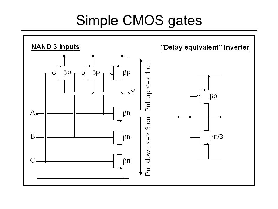
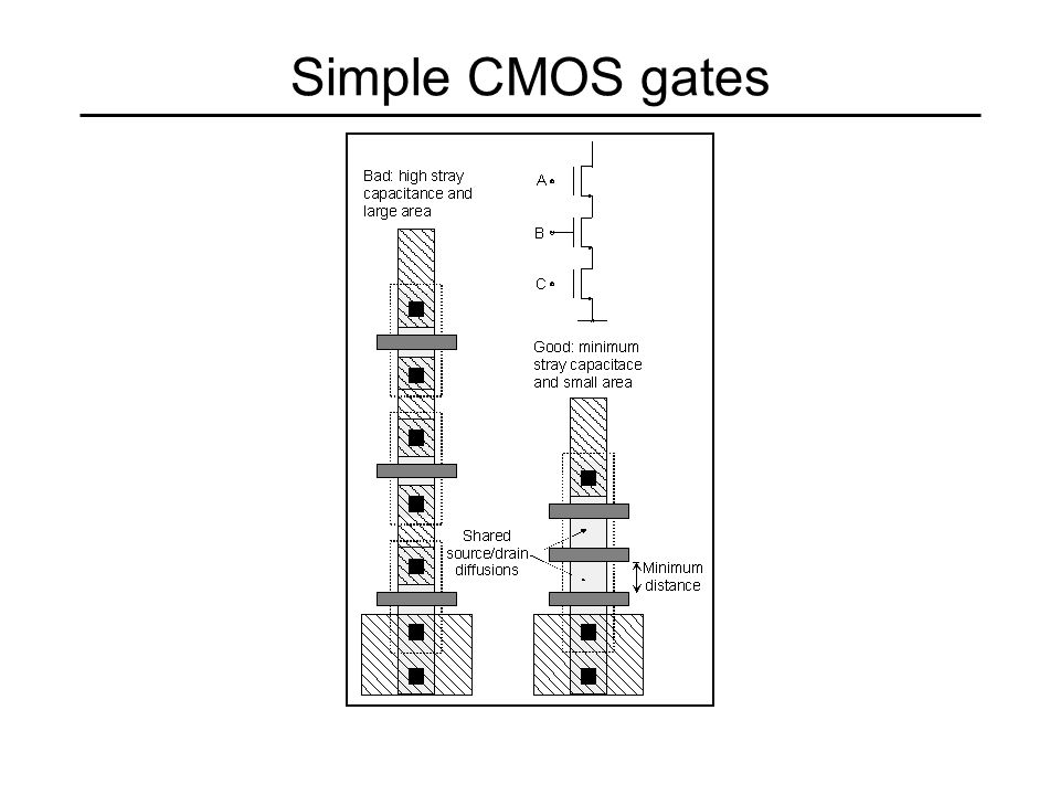
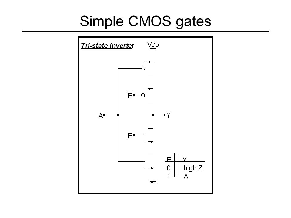
Simple CMOS gates

17
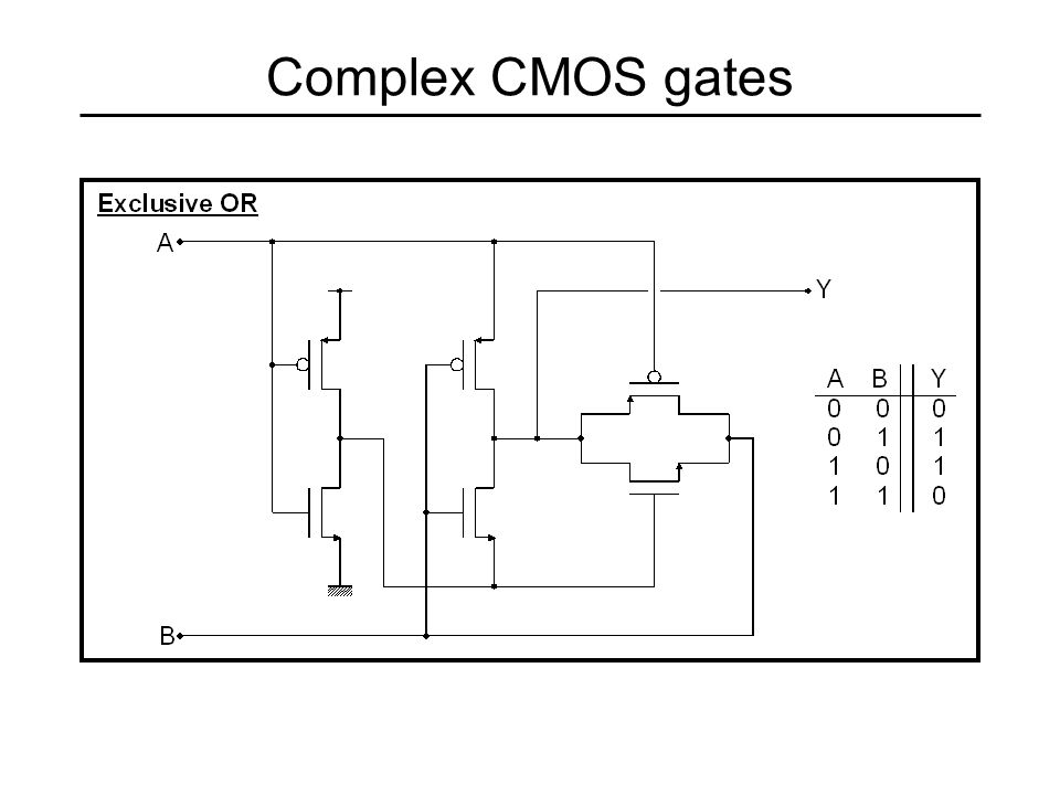
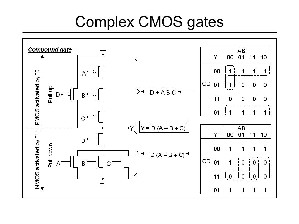
Complex CMOS gates

21
Can a compound gate be arbitrarily complex? –NO, propagation delay is a strong function of fan- in: –FO Fan-out, number of loads connected to the gate: 2 gate capacitances per FO + interconnect –FI Fan-in, Number of inputs in the gate: Quadratic dependency on FI due to: –Resistance increase –Capacitance increase –Avoid large FI gates (Typically FI 4)
.")
22
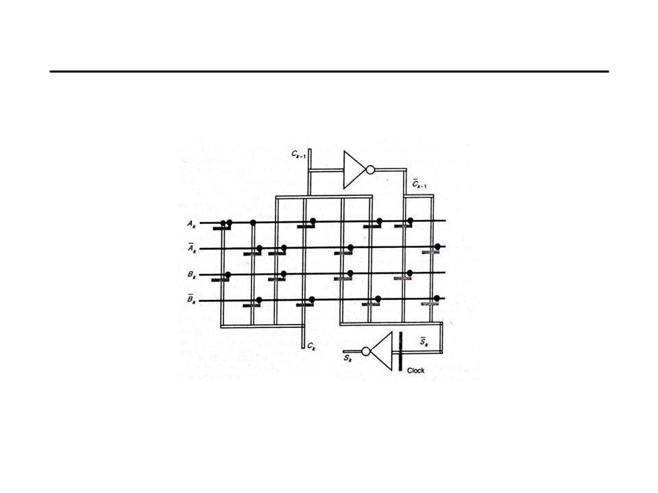
Single-Bit Addition Half Adder Full Adder ABC out S 0000 0101 1001 1110 AkAk BkBk C k-1 CkCk SkSk 00000 00101 01001 01110 10001 10110 11010 11111 For the Sum S k If A k =B k then Sk=C k-1 else S k =C k-1 For the carry If A k =B k then C k =A k =B k else C k =C k-1

28
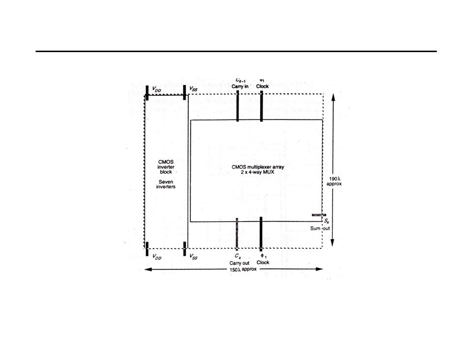
17: Adders 28 Full Adder Design I Brute force implementation from eqns

29
17: Adders 29 Full Adder Design II Factor S in terms of C out S = ABC + (A + B + C)(~C out ) Critical path is usually C to C out in ripple adder
(~C out ) Critical path is usually C to C out in ripple adder")
30
Complex CMOS gates

Similar presentations


![COMBINATIONAL LOGIC [Adapted from Rabaey’s Digital Integrated Circuits, ©2002, J. Rabaey et al.]](/7/1652107/big_thumb.jpg "COMBINATIONAL LOGIC [Adapted from Rabaey’s Digital Integrated Circuits, ©2002, J. Rabaey et al.]>")


