Download presentation
Presentation is loading. Please wait.

1
CHAPTER 9 MULTIPLEXERS, DECODERS, AND PROGRAMMABLE LOGIC DEVICES
9.1 Introduction 9.2 Multiplexers 9.3 Three-State Buffers 9.4 Decoders and Encoders 9.5 Read-Only Memories 9.6 Programmable Logic Devices 9.7 Complex Programmable Logic Devices 9.8 Field Programmable Gate Arrays

2
Objectives 1. Explain the function of a multiplexer. Implement a multiplexer using gates. 2. Explain the operation of three-state buffers. Determine the resulting output when three-state buffers outputs are connected together. Use three-state buffers to multiplex signals onto a bus. 3. Explain the operation of a decoder and encoder. Use a decoder with added gates to implement a set of logic functions. Implement a decoder or priority encoder using gates. 4. Explain the operation of a read-only memory (ROM). Use a ROM to implement a set of logic functions. 5. Explain the operation of a programmable logic array (PLA). Use a PLA to implement a set of logic functions. Given a PLA table or an internal connection diagram for a PLA, determine the logic functions realized. 6. Explain the operation of a programmable array logic device (PAL). Determine the programming pattern required to realize a set of logic function with a PAL. 7. Explain the operation of a complex programmable logic device (CPLD) and a field programmable gate array (FPGA). 8. Use Shannon’s expansion theorem to decompose a switching function.
. Use a ROM to implement a set of. logic functions. 5. Explain the operation of a programmable logic array (PLA). Use a PLA to implement. a set of logic functions. Given a PLA table or an internal connection diagram for a PLA, determine the logic functions realized. 6. Explain the operation of a programmable array logic device (PAL). Determine the programming pattern required to realize a set of logic function with a PAL. 7. Explain the operation of a complex programmable logic device (CPLD) and a field. programmable gate array (FPGA). 8. Use Shannon’s expansion theorem to decompose a switching function.")
3
9.1 Introduction Multiplexer, Decoder, encoder. Three-state Buffer
ROMs PLD PLA CPLD FPGA

4
9.2 Multiplexers Fig to-1 Multiplexer and Switch Analog

5
9.2 Multiplexers Fig 9-2. Multiplexer (1)
")
6
9.2 Multiplexers Fig 9-2. Multiplexer (2)
")
7
9.2 Multiplexers Fig 9-2. Multiplexer (3)
")
8
9.2 Multiplexers Fig 9-3. Logic Diagram for 8-to-1 MUX

9
9.2 Multiplexers Fig 9-4. Quad Multiplexer Used to Select Data

10
9.2 Multiplexers Fig 9-5. Quad Multiplexer with Bus Inputs and Output

11
9.3 Three-State Buffers Fig 9-6. Gate Circuit with Added Buffer

12
9.3 Three-State Buffers Fig 9-7. Three-State Buffer

13
9.3 Three-State Buffers Fig 9-8. Four Kinds of Three-State Buffers B A
C 0 0 0 1 1 0 1 1 Z 1 B A C 0 0 0 1 1 0 1 1 Z 1 B A C 0 0 0 1 1 0 1 1 1 Z B A C 0 0 0 1 1 0 1 1 1 Z (a) (b) (c) (d)
 (b) (c) (d)")
14
9.3 Three-State Buffers Fig 9-9. Data Selection Using Three-State Buffers

15
9.3 Three-State Buffers Fig 9-10. Circuit with Two Three-State Buffers
X S2 1 Z X = Unknown

16
9.3 Three-State Buffers Fig Bit Adder with Four Sources for One Operand

17
9.3 Three-State Buffers Fig Integrated Circuit with Bi-Directional Input/Output Pin

18
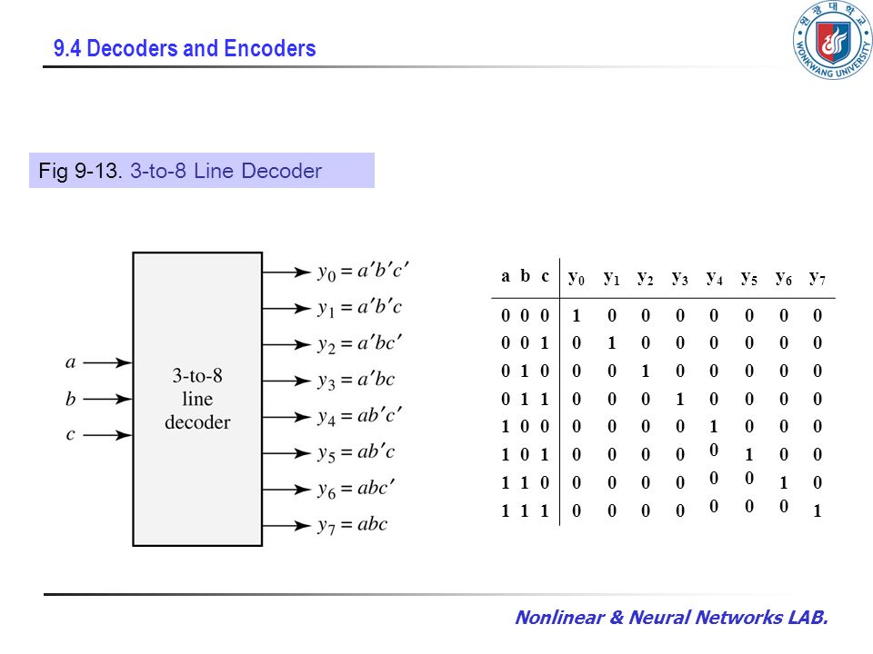
9.4 Decoders and Encoders Fig 9-13. 3-to-8 Line Decoder a b c y0 y1 y2
1 10
19
9.4 Decoders and Encoders Fig A 4-to-10 Line Decoder (1)
")
20
9.4 Decoders and Encoders Fig 9-14. A 4-to-10 Line Decoder (2)
BCD Input Decimal Output A B C D 1 2 3 4 5 6 7 8 9 11 Fig A 4-to-10 Line Decoder (2) (c) Truth Table
 (c) Truth Table.")
21
9.4 Decoders and Encoders Fig Realization of a Multiple-Output Circuit Using a Decoder

22
9.4 Decoders and Encoders Fig 9-16. 8-to-3 Priority Encoder y0 y1 y2
b c d 1 X 01

23
9.5 Read-Only Memories Fig 9-17. An 8-Word x 4-Bit ROM A B C F0 F1 F2
1 typical data stored in ROM (23 words of 4bits each) (a) Block diagram (b) Truth table for ROM
 (a) Block diagram. (b) Truth table for ROM.")
24
9.5 Read-Only Memories Fig Read-Only Memory with n Inputs and m Outputs n input Variables m output 00 11 · · · · 01 10 100 010 101 110 001 011 111 000 typical data array stored in ROM (2n words of m bits each)
")
25
9.5 Read-Only Memories Fig Basic ROM Structure

26
9.5 Read-Only Memories Fig An 8-Word x 4-Bit ROM

27
9.5 Read-Only Memories Fig Equivalent OR Gate for F0

28
ASCII Code for Hex Digit
9.5 Read-Only Memories Fig Hexadecimal to ASCII Code Converter Input Hex Digit ASCII Code for Hex Digit W X Y Z A6 A5 A4 A3 A2 A1 A0 1 2 3 4 5 6 7 8 9 A B C D E F

29
9.5 Read-Only Memories Fig ROM Realization of Code Converter

30
9.6 Programmable Logic Devices
Fig Programmable Logic Array Structure

31
9.6 Programmable Logic Devices
Fig PLA with Three Inputs, Five Product Terms, and Four Outputs

32
9.6 Programmable Logic Devices
Fig AND-OR Array Equivalent to Figure 9-25

33
9.6 Programmable Logic Devices
Table 9-1. PLA Table for Figure 9-25 Product Term Inputs Outputs A B C F0 F1 F2 F3 A’B’ AC’ BC’ AC 1 -

34
9.6 Programmable Logic Devices
Fig PLA Realization of Equations (7-23b) a b c d f1 f2 f3 1 - (a) PLA table
 a. b. c. d. f1. f2. f (a) PLA table.")
35
9.6 Programmable Logic Devices
Programmable Array Logic The symbol of Figure 9-28(a) logically equal
 logically equal.")
36
9.6 Programmable Logic Devices
Programmable Array Logic Connections to the AND gate inputs in a PAL

37
9.6 Programmable Logic Devices
Fig PAL Segment

38
9.6 Programmable Logic Devices
Fig Implementation of a Full Adder Using a PAL

39
9.7 Complex Programmable Logic Devices
Fig Architecture of Xilinx XCR3064XL CPLD (Figure based on figures and text owned by Xilinx, Inc., Courtesy of Xilinx, Inc. © Xilinx, Inc All rights reserved.)
")
40
9.7 Complex Programmable Logic Devices
Fig CPLD Function Block and Macrocell (A Simplified Version of XCR3064XL)
")
41
9.8 Field Programmable Gate Arrays
Fig Equivalent OR Gate for F0

42
9.8 Field Programmable Gate Arrays
Fig Simplified Configurable Logic Block (CLB)
")
43
9.8 Field Programmable Gate Arrays
Fig Implementation of a Lookup Table (LUT) a b c d f 1
 a. b. c. d. f. 1.")
44
9.8 Field Programmable Gate Arrays
Decomposition if switching Functions

45
9.8 Field Programmable Gate Arrays
Decomposition if switching Functions

46
9.8 Field Programmable Gate Arrays
Fig Function Expansion Using a Karnaugh Map

47
9.8 Field Programmable Gate Arrays
Fig Realization of Five- and Six-Variable Functions with Function Generators

Similar presentations


 Personalized by making or breaking.>")

 – –a fixed array of AND gates.>")


 The slides included herein were taken.>")

 Fixed OR array programmable AND array Fixed OR array programmable AND array Easy to program Easy to program Poor flexibility.>")

