Download presentation
Presentation is loading. Please wait.

1
The crystal structure of the III-V semiconductors
Diamond and Zincblende Lattices Unit cells for silicon (Si) and gallium arsenide (GaAs) Silicon - diamond lattice GaAs - zincblende (cubic zinc sulfide) lattice (most other III-V and many II-VI semiconductors have zincblende lattice)Diamond and zincblende lattice based on tetragonal pattern of bonds from each atom to nearest neighbors-two interlocking facecentered- cubic lattices lattice parameter (or constant), a- repeat length of the unit cells e. g., GaAs, a = 5.65 Å (Angstroms) = nm.
 and gallium arsenide (GaAs) Silicon - diamond lattice GaAs - zincblende (cubic zinc sulfide) lattice (most other III-V and many II-VI semiconductors have zincblende lattice)Diamond and zincblende lattice based on tetragonal pattern of bonds from each atom to nearest neighbors-two interlocking facecentered- cubic lattices lattice parameter (or constant), a- repeat length of the unit cells. e. g., GaAs, a = 5.65 Å (Angstroms) = nm.")
2
The band structure ?

3
First Brillouin zone E vs. k band diagram of zincblende semiconductors
One relevant conduction band is formed from S- like atomic orbitals “unit cell” part of wavefunction is approximately spherically symmetric. The three upper valence bands are formed from (three) P- like orbitals and the spin-orbit interaction splits off lowest, “split-off” hole (i. e., valence) band. The remaining two hole bands have the same energy (“degenerate”) at zone center, but their curvature is different, forming a “heavy hole” (hh) band (broad), and a “light hole” (lh) band (narrower)
 P- like orbitals. and the spin-orbit interaction splits off. lowest, split-off hole (i. e., valence) band. The remaining two hole bands. have the same energy ( degenerate ) at zone center, but their curvature is. different, forming a heavy hole (hh) band (broad), and a light hole (lh) band (narrower)")
4
Compound Semiconductors (alloys)
For optoelectronics, most devices are fabricated of“compound semiconductors” particularly III-V materials made from •Group III (Al, Ga, In) and •Group V (N, P, As, Sb) elements •Sometimes Si and Ge (Group IV) are used as photodetectors •Sometimes II-VI (e.g. ZnSe) and IV-VI materials (e.g., PbTe) Alloys of compound semiconductors used extensively to adjust the basic materials properties, e.g., lattice constant, bandgap,refractive index, optical emission or detection wavelength EXAMPLE – InxGa1- xAs (where x is the mole fraction of indium) InxGa1- xAs is not strictly crystalline because not every unit cell is identical (random III site location), but we treat such alloys as crystalline to a first approximation
 and. •Group V (N, P, As, Sb) elements. •Sometimes Si and Ge (Group IV) are used as photodetectors. •Sometimes II-VI (e.g. ZnSe) and IV-VI materials (e.g., PbTe) Alloys of compound semiconductors used extensively to adjust the basic materials properties, e.g., lattice constant, bandgap,refractive index, optical emission or detection wavelength. EXAMPLE – InxGa1- xAs (where x is the mole fraction of indium) InxGa1- xAs is not strictly crystalline because not every unit cell. is identical (random III site location), but we treat such alloys as. crystalline to a first approximation.")
5
The Human eye response Lasers and LEDs for displays or lighting must emit in the nm wavelength region (bandgaps of eV).
.")
6
Technologically Available Materials

7
Some of the applacations
Large Area, Full Color Displays LED Traffic Lights

8
the first principles calculation guess first
compare charge convergence new

9
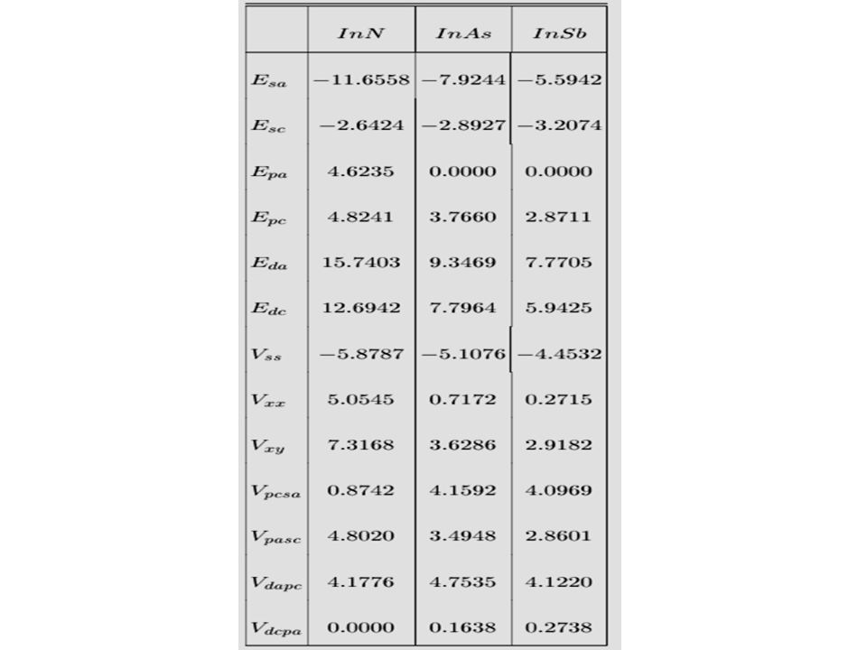
Empirical tight binding
Hv= < |Hv-ESv|= 0

10
The Hamiltonian in sp3d2

11
The equation came from ETB

12
Volume optimization for InN by wien2K

13
Volume optimization for InAs by wien2K

14
Volume optimization for InSb by wien2K

15
Band structure of InN by wien2k

16
Band structure of InAs by wien2k

17
Band structure of InSb by wien2k

18
Band structure of InN by ETB

19
Density of states for InN

20
Band structure of InAs by ETB

21
Density of states for InAs

22
Band structure of InSb by ETB

23
Density of states for InSb

Similar presentations


 Computers –Human based –Tube based –Solid state based Why do we need computers? –Modeling Analytical- great.>")
>")


