Download presentation
Presentation is loading. Please wait.

1
Advanced Process Integration
ECE 7366 Advanced Process Integration The CMOS Traasistors Dr. Wanda Wosik Text Book: B. El-Karek, “Silicon Devices and Process Integration”, Chapter 5

2
FET Structures

4
Non-Ideal MOS Structure
Work function difference vs doping for Al gates and degenerate poly-silicon p+ and n+ type. Note the symmetry of fms for poly-Si and asymmetry for Al gates Band bending due to work function differences. No charge in the oxide assumed

5
Polysilicon Workfunction
Intrinsic Si The role of Ge in regulating work function of polysilicon: p+ polySi by 0.4eV (strain for higher Ge x>0.45). Less doping (VG )– higher mobility
. Less doping (VG )– higher mobility.")
6
Scaled down NMOS device with poly-Si gate
Poly-Si depletion Inversion capacitance decreases Charging at the metal dielectric interface Dipol EF,m aligns more with ECNL,d it is increasingly more (S to 0 for perfect pinning) with increasing e of dielectric Effective work function Fm changes from the metal vaccuum level Yeo,IEEE, 2002
 with increasing e of dielectric Effective work function Fm changes from the metal vaccuum level. Yeo,IEEE,")
7
Selection of Metal Gates and High-K Dielectric
obtained required Use dual work function metal gates Stability of work function on dielectric: Silicon Nitrides of Ti, Ta Watch for resistivity. Y-C Yeo et al.

8
Effect of Fermi level pinning
is smaller for poly-si gates – less changes of effective work function Metal F-level pinned to ECNL of the dielectric. Yeo, IEEE 2002

9
Metal Gates Midgap work function: W, TiN, W/TiN ~4.8 eV ~4.7 eV
Disadvantage in small devices: high concentrations in the channel ~1018cm-3 (fb~0.5eV ) VT~0.5V but VT required ~ V (VG-VT). To lower VT use implant (buried channel devices)– bad for mobility & SCE so midgap gates are not good for scaled down devices. Dual work function: c+0.2V (NMOS) ~ 4.35eV and c+Eg/q-0.2V (PMOS) 5.07 eV ~4.7 eV Yang et al. Y-C Yeo et al.
 VT~0.5V but VT required ~ V (VG-VT). To lower VT use implant (buried channel devices)– bad for mobility & SCE so midgap gates are not good for scaled down devices. Dual work function: c+0.2V (NMOS) ~ 4.35eV and c+Eg/q-0.2V (PMOS) 5.07 eV. ~4.7 eV. Yang et al. Y-C Yeo et al.")
11
Work Function Requirements and Options
~0.4 eV for UT SOI Verghese, SST, 2012

12
Metal gates – challenge to control work function and stability
Polishchuk, 2001

13
Fully Silicided Gate FUSI
Fermi Level Pinning For metal gates metal induced surface states MIGS Fully Silicided Gate FUSI NiSi doped with As (4.58 eV), B (5.1. eV), or undoped poly_Si (4.87 eV) – doping changes the workfunction NixSiy &phase change the workfuction as well 4.44 eV 5.0 eV
, B (5.1. eV), or undoped poly_Si (4.87 eV) – doping changes the workfunction. NixSiy &phase change the workfuction as well 4.44 eV 5.0 eV.")
14
Frank&Taur, SSE, 2002

15
Process Flow for ICs Define; components their parameters tolerances
limitations range of operating T reliability tools and limitations in production overall costs Define process flow simulate devices and processes run experimental short-loops use test structures design, simulate and process complete test structure that includes process monitoring components’ parameters testing their tolerances & reliability yield structure

16
A Conventional CMOS Logic Process Flow - STI
Depth~ µm nm Etch oxide for easier CMP 10-20nm cm-3 epi 1019cm-3 (100) Nitride is the stop layer 10-15nm
 Nitride is the stop layer nm.")
17
A Conventional CMOS Logic Process Flow – Well implants
Oxide&nitride pads removed; grow P-well for NMOS will be similarly done by Implantation Tailored profile in Implantation Oxide is used to decrease channeling effect in implantation &protect the surface

18
A Conventional CMOS Logic Process Flow – gates/junctions/contacts
Sacrificial oxide etched Gate oxide grown 3-4 nm Undoped poly-Si grown PolySi patterned by RIE Pattern NMOS vs PMOS Implant S/D & gate Thin oxide on poly removes RIE damage and protects gate in P/As implant Halo implants Remove oxide and sputter deposit ~20-30nm metal: Ti, Co Ni ox~10-15 nm CVD deposition and etch back of nitride nm Poly-Si gate doping: single workfunction (ex. P – watch for VT in PMOS that gives buried channel) dual workfunction (ex. B outdiffusioncan also lead to buried channels PMOS) watch for poly-Si depletion Watch for junction leakage due to silicon consumption during silicidation
 dual workfunction (ex. B outdiffusioncan also lead to buried channels PMOS) watch for poly-Si depletion. Watch for junction leakage due to silicon consumption during silicidation.")
19
A Few Notes on Spacers Park &Hu

21
Niwa, Sematech Symposium

22
What we Gain by Using Metal Gates
Hoffmann,SST, 2010

23
Metal Gates Gate first or gate last=replacement-gate? CMP

24
Dual Metal Gate for High CMOS Performance
Process Flow Niwa, Sematech Symposium Yeo, IEEE, 2004

25
Dual Work Function Gates
10 nm 5 nm 20 nm For PMOS use Ru as a gate electrode LOCOS replaced by STI 20 nm

26
Metal Interdiffusion Approach Single Metal Doping Approach
(Ti~4eV) Decreased to ~4.5eV ~5eV (Ni~5eV) Yeo, IEEE, 2004
 Decreased to. ~4.5eV. ~5eV. (Ni~5eV) Yeo, IEEE,")
27
Dual Workfunction Metal Gate Process
Reactive sputtering TiN wet etch ALD Reactive Sputtering of TaSiN Heavy doped

28
Gate Stacks in High-K/Metal Gate System
Niwa, Sematech Symposium

29
Fully Silicided Polysilicon FUSI
Earlier shown for CoSi nm Workfunction modified by Ni/Si ratio: Si-rich fm~4.5 eV (NMOS) Ni-rich fm~4.85 eV (PMOS) Silicidation can be done for NMOS and PMOS Dopant concentration changes work function Use M1 at the gate & other metal M2 on top
 Ni-rich fm~4.85 eV (PMOS) Silicidation can be done for NMOS and PMOS. Dopant concentration changes work function. Use M1 at the gate & other metal M2 on top.")
30
FUSI Using Ni-Silicidation on Doped Poly Si
As and B doping Changes of WF values by As (snow plow) but not by B Maszara et al. IEEE 2002
 but not by B. Maszara et al. IEEE")
31
FUSI – Limitations NMOS for different silicidation
NMOS gate leakage larger for FUSI than for Poly-SI gate

32
FUSI using Amorphous Si and Ni-Silicide
The role of oxygen (measure profiles) in incomplete silicidation 400°C/5min 100nm 900°C/20min 6-19nm HP Yu et al., 2006
 in incomplete silicidation. 400°C/5min. 100nm. 900°C/20min. 6-19nm. HP Yu et al.,")
33
Doped and Undoped Poly-Si (950°/10s)
Phase Controlled FUSI Doped and Undoped Poly-Si (950°/10s) Dielectrics: HfSiON and SiO2 ~4.5eV ~4.8eV ~4.4eV ~4.8eV ~4.4eV ~4.5eV No degradation of h&el mobility Takalashi et al. IEDM, 2004
 Dielectrics: HfSiON and SiO2. ~4.5eV. ~4.8eV. ~4.4eV. ~4.8eV. ~4.4eV. ~4.5eV. No degradation of h&el mobility. Takalashi et al. IEDM,")
34
Metal Gates - Deposition (ALD) of Metallic Films
H. Kim, Sematech Mtg, 2012

35
FLP effect interface dipoles change EWF
Measurements done on variable oxide thickness Eizenberg and Kornblum, Sematech Mtg.

36
Interfacial layers change EWF
Use Capping Layers K=8 Another example: Hf NMOS & HfNxPMOS HfNx gate (N/Hf ratio 0 to 2) Interface from processing issues (reactive sputtering etc.) Interfacial layer increases EWF of Ta Al & P have EWF as in vacuum Rothschild, Sematech Mtg.
 Interface from processing issues (reactive sputtering etc.) Interfacial layer increases EWF of Ta. Al & P have EWF as in vacuum. Rothschild, Sematech Mtg.")
37
Capping Layers for Interfacial Charges/WF Control Constrains
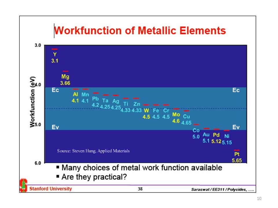
Niwa, Sematech Symposium Caps are added on purpose to set the WF due to dipoles – stability? – reliability? Planar Replacement Gate Device Structure Verghese, SST, 2012

38
EWF in PMOS with caps roll to mid-gap upon annealing
Gate first: Al2O3 for PMOS and LaOx for NMOS used as thin capping layers for dipoles that would determine VT – Instability – roll-off. EWF higher than in MIPS (metal inserted poly-Si) Hoffmann,SST, 2010
 Hoffmann,SST,")
39
Niwa, Sematech Symposium

41
Small Size Effects Important: size calls for N in the substrate fluctuation in doping fluctuation fluctuation in VT – problems for circuits (analog more than digital)
")
42
Gate Stack History of gates in MOSFETs: metal gate Al – not self aligned polysilicon n+ type dual poly-gates silicides poly-gates fully silicidedpoly-gates metal gates – midgap metal gates – dual

43
High-k + Metal Gate Benefits
High-k gate dielectric Reduced gate leakage TOX(e) scaling Metal gates Eliminate polysilicon depletion Resolves VT pinning and poor mobility for high-k dielectrics Kawanago, PhD, 08D36028
 scaling. Metal gates. Eliminate polysilicon depletion. Resolves VT pinning and poor mobility for high-k dielectrics. Kawanago, PhD, 08D")
44
Kawanago, PhD, 08D36028

45
Gate Stack Module Gates scaling movie
Poly-Si depletion ~1.2 nm CET by ~ 0.4 nm Poly-Si leaks B to the channel (dielectric and Si) Gate-stack transition from silicides, doped poly-Si on SiO2 to metal gates on high-K dielectric Gates scaling movie Hsing-Huang Tseng
 Gate-stack transition from silicides, doped poly-Si on SiO2 to metal gates on high-K dielectric. Gates scaling movie. Hsing-Huang Tseng.")
46
Iwai

Similar presentations


. Diffusion Process The process of materials move from high concentration regions to low concentration regions,>")


 Active (clear field)>")


