Download presentation
Presentation is loading. Please wait.

1
GridPix/Gossip for ATLAS SCT Upgrade ILC CLIC
…….insulators in strong E- fields………. …….the frustration of innovation……….. Harry van der Graaf Nikhef, Amsterdam IEEE-NSS Conference MPGD-Si Detector Workshop Dresden, Oct 18, 2008

2
Micro Strip Gas Counters: hard to operate:
discharges, ruining electrodes ageing ! Very strong electric field in insulator’s volume & surface !

3
GEMs: often cascade of 3 GEMs used to limit gain per GEM to ~40 ‘rim’ (dia hole Cu/kapton) critical shape of hole wall critical charge up effects

4
Overview of MPGD development in JAPAN
Atsuhiko OCHI Kobe University, JAPAN 13 Oct nd RD51 workshop in Paris

5
GEM Production Remove copper by wet etching Irradiate CO2 laser
Recent Status of Development GEM Production RIKEN/SciEnergy GEM (thick-foil and fine-pitch) pitch 80um hole 40um thickness 100um 100um 80um x750 Remove copper by wet etching Irradiate CO2 laser Remove remaining edge from the other side 5
 pitch 80um. hole 40um. thickness 100um. 100um. 80um. x750. Remove copper. by wet etching. Irradiate CO2 laser. Remove remaining edge from the other side. 5.")
6
Recent Status of Development
Gain Curve (RIKEN GEM) GEM test setup and parameters Thick-foil and fine-pitch GEM (single layer) HV supplied through a resister chain Ed=2.5kV/cm, Ei=4~5kV/cm, ⊿VGEM=300~600V Gas: Ar+CO2(30%) flow Readout by 1cm x 1cm pad Gain measurement Gain vs applied voltage X-ray from Fe-55 (5.9keV) Fe-55 spectrum 5.9keV gain=3x10⁴ To keep good spatial resolution and keep discharge point at high gain. Our GEM is most suitable for Cosmic X-ray Polarimeters. 6
 GEM test setup and parameters. Thick-foil and fine-pitch GEM. (single layer) HV supplied through a resister chain. Ed=2.5kV/cm, Ei=4~5kV/cm, ⊿VGEM=300~600V. Gas: Ar+CO2(30%) flow. Readout by 1cm x 1cm pad. Gain measurement. Gain vs applied voltage. X-ray from Fe-55 (5.9keV) Fe-55 spectrum. 5.9keV. gain=3x10⁴. To keep good spatial resolution and keep discharge point at high gain. Our GEM is most suitable for Cosmic X-ray Polarimeters. 6.")
7
Gain instability (RIKEN GEM)
Recent Status of Development Gain instability (RIKEN GEM) No increase and decrease just after HV on. F. Simon (IEEE, 2006) T. Tamagawa(IEEE,2007) time (s) relative gain 3 hours No gain increase in short measurements This is not for a special batch of GEMs but for all GEMs we produced Possible reasons; Less charging-up due to cylindrical hole shape Less polarization of Liquid Crystal Polymer 7
 No increase and decrease just after HV on. F. Simon (IEEE, 2006) T. Tamagawa(IEEE,2007) time (s) relative gain. 3 hours. No gain increase in short measurements. This is not for a special batch of GEMs but for all GEMs we. produced. Possible reasons; Less charging-up due to cylindrical hole shape. Less polarization of Liquid Crystal Polymer. 7.")
8
GemGrid 1 GemGrid 2

9
Bulk high-resistivity materials
hydregenated amorphous silicon allowed gains up to 5 105 staying proportional! Si-rich silicon nitride (Si3N4)
")
10
Measurements on Si-rich Silicon Nitride (Si3N4)
Column resistance: ρ D/O Potential surface measurable: gain drop factor 2 at dV = 17.5 V With known current: bulk resistivity ρ measurable: ~ 1 – Ohm cm Surface time constant: Column resistance x (virtual colum capacitance) = (ρ D/O)*(ε O/D) = ρ ε (independant of layer thickness D!)
 = (ρ D/O)*(ε O/D) = ρ ε (independant of layer thickness D!)")
11
Resistive Plate Chambers (RPCs)
essential: high-resistivity material - quenches sparks - sufficient charge compensation current Traditional: insulator + dope (Sardinian oils…?) New: high-resistivity bulk (ceramic) material: higher counting rates Compare graphite covered mylar foil
 New: high-resistivity bulk (ceramic) material: higher counting rates. Compare graphite covered mylar foil.")
12
conductivity of kapton
Micromegas on pillars Edge discharge protection foil discharges + vibrations

14
Charge-up effects After (rapid) ramping of HV: polarisation: reduction of E-field in insulator (bulk) volume In homogeneous field with insulator // to field: nothing With E component perp. on insulating surface: modification of potential by hitting e- and/or ions until E // surface

15
GEM hole

16
equalizing with water Stronger effects for good insulator region of worse insulation

17
Very preliminary: Use as little as possible insulating surfaces // strong E fields Apply high-resistivity materials instead of insulators Even more preliminary: As for gain: GEMs perform les than (corresponding) Micromegas
 Micromegas.")
18
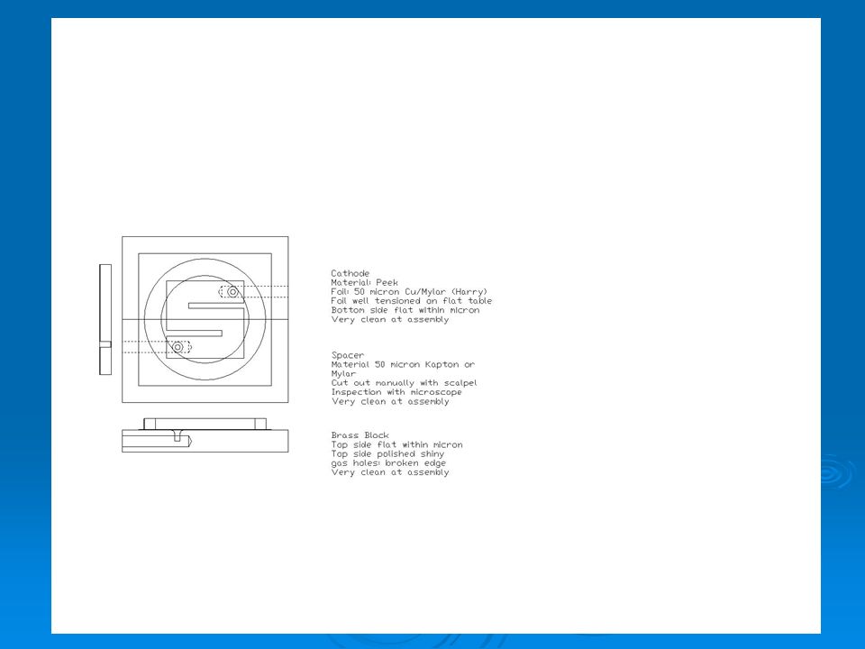
MIPs April 2004 Micromegas + MediPix 2 NIKHEF/Saclay/Univ. Twente:
No source, 1s 55Fe, 1s 55Fe Cathode (drift) plane Drift space: 15 mm Micromegas Baseplate MediPix2 pixel sensor Brass spacer block Printed circuit board Aluminum base plate 14 mm δ-ray! He/Isobutane 80/20 Modified MediPix MIPs
 plane. Drift space: 15 mm. Micromegas. Baseplate. MediPix2 pixel sensor. Brass spacer block. Printed circuit board. Aluminum base plate. 14 mm. δ-ray! He/Isobutane. 80/20. Modified MediPix. MIPs.")
19
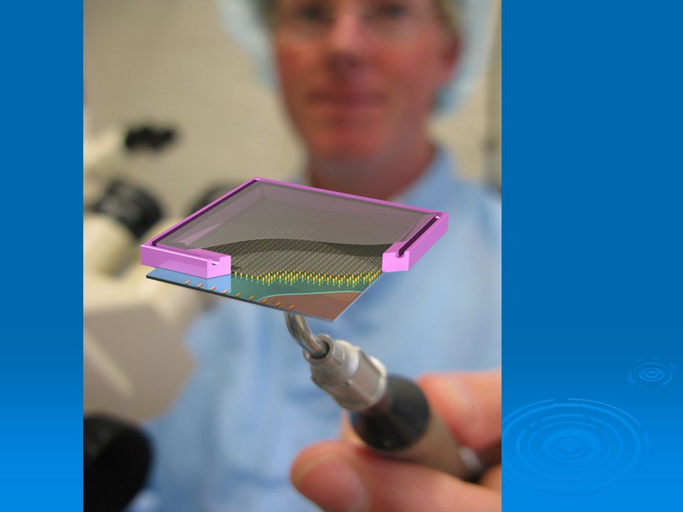
‘wafer post processing’
Integrate Micromegas and pixel sensor: InGrid ‘wafer post processing’ by Univ. of Twente, MESA+’

20
Full post-processing of a TimePix
Timepix chip + SiProt + Ingrid: 14 mm MESA+ “Uniform” IMT Neuchatel Charge mode

21
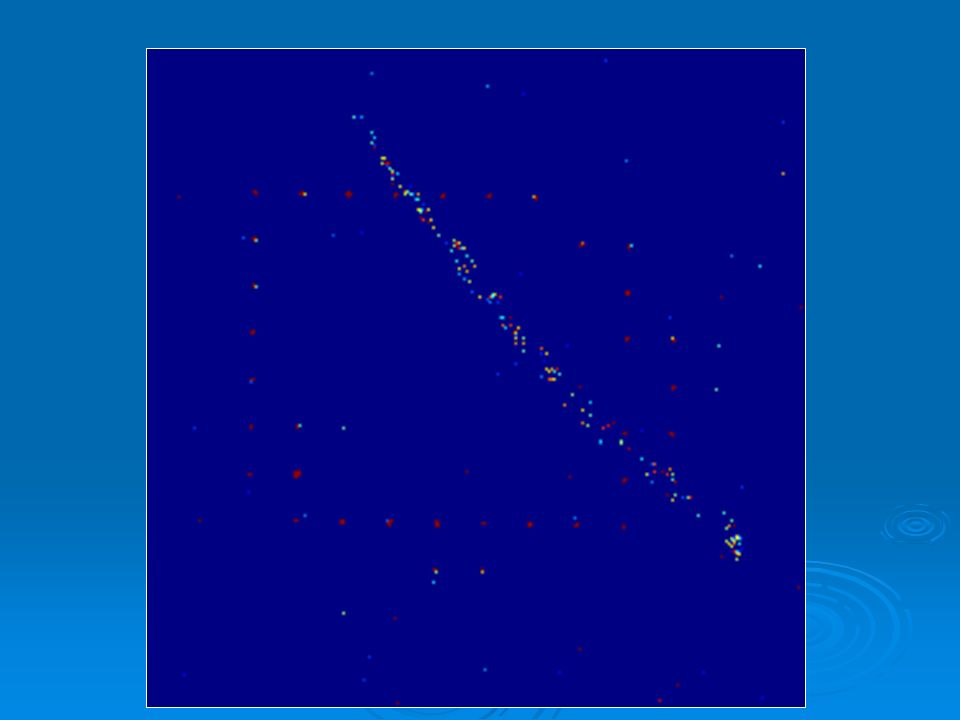
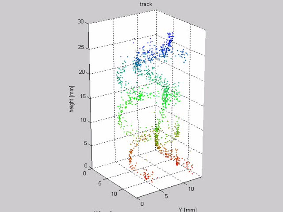
A “long” cosmic track Timepix + 20 μm thick Siprot Ingrid
cathode @ V 14 mm 10 mm A “long” cosmic track Timepix + 20 μm thick Siprot Ingrid Drifttime (bin = 10 ns) Stable operation in He iC4H10
 Stable operation in He iC4H10.")
23
Si (vertex) track detector GOSSIP
Cluster3 Cathode (drift) plane Integrated Grid (InGrid) Cluster2 Cluster1 Slimmed Silicon Readout chip Input pixel 1mm, 100V 50um, 400V 50um CMOS chip Si depletion layer Vbias Gas: 1 mm as detection medium 99 % chance to have at least 1 e- Gas amplification ~ 1000: Single electron sensitive All signals arrive within 16 ns Si strip detectors Si pixel detectors MAPs
 plane. Integrated Grid (InGrid) Cluster2. Cluster1. Slimmed Silicon Readout chip. Input pixel. 1mm, 100V. 50um, 400V. 50um. CMOS chip. Si depletion layer. Vbias. Gas: 1 mm as detection medium. 99 % chance to have at least 1 e- Gas amplification ~ 1000: Single electron sensitive. All signals arrive within 16 ns. Si strip detectors. Si pixel detectors. MAPs.")
24
Gossip: replacement of Si tracker Essential: thin gas layer (1.2 mm)
![]()
25
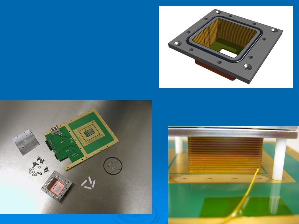
GOSSIP-Brico: PSI-46 (CMS Pixel FE chip)
First prototype of GOSSIP on a PSI46 is working: • 1.2 mm drift gap • Grid signal used as trigger • 30 µm layer of SiProt
![]()
26
Tracking sensor material: gas versus Si
it is light primary electrons can simply be multiplied: gas amplification: low power no bias current: low power & simple FE circuits gas can be exchanged: no radiation damage of sensor gas has a low εr: with small voxels the source capacity can be small (10 fF) allowing fast, low-noise, and low-power preamps gas is usually cheap low sensitive for neutron and X-ray background δ-rays can be recognized [high ion & electron mobility: fast signals, high count rates are possible] discharges/sparks: readout system should be spark proof ageing: must be solved and must be understood / under control diffusion: limits max. drift length
![]()
27
Silicon Protection: SiProt
CMOS Chip protection against - discharges - sparks - HV breakdowns - too large signals Silicon Protection: SiProt Amorph Si (segmented) Emperical method: Try RPC technology
 Emperical method: Try RPC technology.")
28
Qmax ~ 1 – 2 fC Chip may die if Qmax > 10 fC

29
Ageing Little ageing expected:
Radiation damage of CMOS pixel chip is relevant - common for all tracking detectors - believed to widthstand ATLAS Upgrade Dose in 90 nm technology Radiation damage of sensor: not relevant for Gossip sensor since this is gas being exchanged Typical for gaseous detectors: the deposit of an (insulating) polymer on the electrodes of a detector. Decrease of signal amplitude Little ageing expected: little primary ionisation (~ 10 e-/track) low gas gain (500 – 1000) large anode surface (compare pixel anode plane with surface of thin wire) E-field at flat anode ~3 lower than E-field at anode wire
 polymer. on the electrodes of a detector. Decrease of signal amplitude. Little ageing expected: little primary ionisation (~ 10 e-/track) low gas gain (500 – 1000) large anode surface (compare pixel anode plane with surface of thin wire) E-field at flat anode ~3 lower than E-field at anode wire.")
30
gas: standard Ar/Methane 90/10. Deposit containing C found on anode

31
Irradiation with 8 keV X-rays: No rate effects up to anode current density of 0.2 μA / mm2 very fast track counting possible! After 0.3 Coulomb/mm2: (eq. 3.7 x 10¹⁶ MIPs/cm2 !!) deposit of carbon polymer on anode is clearly visible. Micromegas is clean (!?) Little deposit on cathode, and…… Chamber still worked! Ageing
 deposit of carbon polymer on anode is clearly visible. Micromegas is clean (! ) Little deposit on cathode, and…… Chamber still worked! Ageing.")
32
Construction of many test chambers
prototypes Next-1,2,3,4,5 Next Quad Next-64 (ReNexed, ReLaXd) DICE Ageing Chambers
 DICE. Ageing Chambers.")
33
Next-64 / ReLaXd / ReNexd CO2 cooling!

34
DICE

35
Reactor Institute Delft RID DICE Nuclear Reactor Water Bassin 10 x 10 x 10 m3

37
Upgraded SCT: Gossip could replace:
Pixel vertex detector: Gossip Si Strip detectors: replace by Gossip Strixel detectors TRT: use Gossip as tracker/TR X-ray detector Essentials: power dissipation: 60 mW/cm2 intrinsic mass: 0.1 % radiation length low cost: 10 $ / cm2

38
Barrel SCT unit EndCap SCT unit

39
Semiconductor (pixel, strip) detectors
Depleted Si, 300 μm Vbias = 150 V electron-hole pairs (pixel) chip with preamps, shapers, discriminators
![]()
40
ATLAS pixel: basic element
C-C support sensor Flex Hybrid bumps MCC Side view not to scale Wire-bonding FE’s Wire-bonding MCC FE chip Flex module 2.x
![]()
41
- Ladder strings fixed to end cones
Integration of beam pipe, end cones & pixel vertex detector 5 double layers seems feasible

42
Gossip in ATLAS (Goat-1) Stave
TimePix-2 chip SiNProt layer InGrid (Si3N4) Gas Cover casted aluminium power line ‘P’(ositive)String carrying 1.3 V ‘G’(round)String gas manifold ‘Road’: C-fibre reinforced databus + aux services StainlessSteel tube for CO2 cooling Stiff, light Stave formed by G-string P-string Road triangle
 Gas Cover. casted aluminium. power line. ‘P’(ositive)String. carrying 1.3 V. ‘G’(round)String. gas. manifold. ‘Road’: C-fibre reinforced databus + aux services. StainlessSteel tube. for CO2 cooling. Stiff, light Stave formed by G-string. P-string. Road triangle.")
43
GOAT: GOssip in ATlas Inner Layer: 7 double Goat strings
Gossip readout Gossip detector unit Ø60mm Beampipe P-string conductor (+voltage) CO2 cooling channels G-string conductor (+voltage)
 CO2 cooling channels. G-string conductor. (+voltage)")
44
Upgraded SCT: Gossip/GridPix could replace:
Pixel vertex detector: Gossip Si Strip detectors: replace by Gossip Strixel detectors TRT: use GridPix as tracker/TR X-ray detector strixels/strips preamp channels ~ 20 mm Essentials: power dissipation: 1/16 x 60 mW/cm2 = 4 mW/cm2 now:25 mW/cm2 intrinsic mass: 0.1 % radiation length low cost: 10 $ / cm2

45
Upgraded Tracker: Gossip could replace:
Pixel vertex detector: Gossip Si Strip detectors: replace by Gossip Strixel detectors TRT: use Gossip with 17 mm Xe layer as tracker/TR X-ray detector Essential: high position-resolution tracker throughout tracker low mass, low cost detector Efficient TRD possible
![]()
46
PS/T9: electrons and pions, 1 – 15 GeV/c
Testbeam Nov 5 – 12, 2007 PS/T9: electrons and pions, 1 – 15 GeV/c L=30 mm V0 V1 f Transition Radiator 0.05 mm Anatoli Romaniouk, Serguei Morozov, Serguei Konovalov Martin Fransen, Fred Hartjes, Max Chefdeville, Victor Blanco Carballo

47
Particle Identification
Samples pions (left) and electrons (right) 6 GeV/c
 and electrons (right) 6 GeV/c.")
48
5 (double) layer Gossip Pixel
4 layer Gossip Strixel radiator 3 layers Gossip TRT
![]()
49
Gas instead of Si Pro: Con:
no radiation damage in sensor: gas is exchanged modest pixel (analog) input circuitry: low power, little space no bias current: simple input circuit CMOS pixel chip main task: data storage & communication (rad hard) low detector material budget: 0.06 % radiation length/layer typical: Si foil. New mechanical concepts low power dissipation : little FE power (2 μW/pixel); no bias dissipation operates at room temperature (but other temperatures are OK) less sensitive for neutron and X-ray background 3D track info per layer if drift time is measured Con: Gaseous chamber: discharges (sparks): destroy CMOS chip gas-filled proportional chamber: ‘chamber ageing’ Needs gas flow Parallax error: 1 ns drift time measurement may be required
 input circuitry: low power, little space. no bias current: simple input circuit. CMOS pixel chip main task: data storage & communication (rad hard) low detector material budget: 0.06 % radiation length/layer. typical: Si foil. New mechanical concepts. low power dissipation : little FE power (2 μW/pixel); no bias dissipation. operates at room temperature (but other temperatures are OK) less sensitive for neutron and X-ray background. 3D track info per layer if drift time is measured. Con: Gaseous chamber: discharges (sparks): destroy CMOS chip. gas-filled proportional chamber: ‘chamber ageing’ Needs gas flow. Parallax error: 1 ns drift time measurement may be required.")
50
New mechanics + cooling concepts for Gossip
As little as possible material detector consists of foil! less power required ( less cooling) w.r.t. Si ‘laundry line’ ‘balloon’ string: power, chip support, cooling in 2030….
 w.r.t. Si. ‘laundry line’ ‘balloon’ string: power, chip support, cooling. in 2030….")
51
Minimum Material Budget
(% rad length) Z = 0 mm Z = +/-600 mm Gossip detector (50 μm Si) Cooling (stainless steel tube) Power (max 0.28 mm aluminium) Data transfer (max 1.7 mm kapton) total angle correction x √ x 2 x √2 3
 Z = 0 mm. Z = +/-600 mm. Gossip detector (50 μm Si) Cooling (stainless steel tube) Power (max 0.28 mm aluminium) Data transfer (max 1.7 mm kapton) total angle correction x √ x 2 x √2 3.")
52
Virtual goal: ATLAS pixel vertex
- Ladder strings fixed to end cones Integration of beam pipe, end cones & pixel vertex detector 5 double layers seems feasible
![]()
54
Gossip in ATLAS (Goat-1) Stave
TimePix-2 chip SiNProt layer InGrid (Si3N4) Gas Cover casted aluminium power line ‘P’(ositive)String carrying 1.3 V ‘G’(round)String gas manifold ‘Road’: C-fibre reinforced databus + aux services StainlessSteel tube for CO2 cooling Stiff, light Stave formed by G-string P-string Road triangle
 Gas Cover. casted aluminium. power line. ‘P’(ositive)String. carrying 1.3 V. ‘G’(round)String. gas. manifold. ‘Road’: C-fibre reinforced databus + aux services. StainlessSteel tube. for CO2 cooling. Stiff, light Stave formed by G-string. P-string. Road triangle.")
55
GOAT: GOssip in ATlas Inner Layer: 7 double Goat strings
Gossip readout Gossip detector unit Ø60mm Beampipe P-string conductor (+voltage) CO2 cooling channels G-string conductor (+voltage)
 CO2 cooling channels. G-string conductor. (+voltage)")
56
The future: Electron Emission Foil MEMS made MicroChannelPlates: 200 ps time resolution: CLIC electron emission foil electron emission foil CMOS pixel chip CMOS pixel chip replace gas by vacuum Micro Channel Plate sub-ns time resolution Note CLIC experiments electron avalanche in gas EE-Foil replaces InGrid Parallel Plate Chamber

58
July 2005: ATLAS Upgrade Worlshop Genua
Contribution Gossip was refused: ……………..pixel B-layer replacement too soon for new R&D projects….. Sept 2006: ATLAS Upgrade Workshop Liverpool: Contribution Gossip was granted (after repeated requests) Dec 2007: ATLAS Upgrade Workshop Valencia: Invited to present Gossip R&D project Sept 2008: PSD8, Glasgow: keynote: Norbert Wermes: Pixel detectors for charges particles mentions 3D, Diamond, MAPs, but NOT Gossip
 Dec 2007: ATLAS Upgrade Workshop Valencia: Invited to present Gossip R&D project. Sept 2008: PSD8, Glasgow: keynote: Norbert Wermes: Pixel detectors for charges particles. mentions 3D, Diamond, MAPs, but NOT Gossip.")
59
Si tracking detectors the ultimate detector in HEP associated with Moore’s Law, chip technology Proposal: (imaginary) separation of Interaction Matter and readout electronics Integration (MAPs) maybe profitable later
![]()
60
Si (vertex) track detector GOSSIP
Cluster3 Cathode (drift) plane Integrated Grid (InGrid) Cluster2 Cluster1 Slimmed Silicon Readout chip Input pixel 1mm, 100V 50um, 400V 50um CMOS chip Si depletion layer Vbias Gas: 1 mm as detection medium 99 % chance to have at least 1 e- Gas amplification ~ 1000: Single electron sensitive All signals arrive within 16 ns Si strip detectors Si pixel detectors MAPs
 plane. Integrated Grid (InGrid) Cluster2. Cluster1. Slimmed Silicon Readout chip. Input pixel. 1mm, 100V. 50um, 400V. 50um. CMOS chip. Si depletion layer. Vbias. Gas: 1 mm as detection medium. 99 % chance to have at least 1 e- Gas amplification ~ 1000: Single electron sensitive. All signals arrive within 16 ns. Si strip detectors. Si pixel detectors. MAPs.")
61
NIKHEF Harry van der Graaf, Max Chefdeville, Fred Hartjes, Jan Timmermans, Jan Visschers, Marten Bosma, Martin Fransen, Yevgen Bilevych, Wim Gotink, Joop Rovekamp University of Twente Cora Salm, Joost Melai, Jurriaan Schmitz, Sander Smits, Victor Blanco Carballo University of Nijmegen Michael Rogers, Thei Wijnen, Adriaan Konig, Jan Dijkema, Nicolo de Groot CEA/DAPNIA Saclay D. Attié, P. Colas, I. Giomataris CERN M. Campbell, X. Llopart University of Neuchatel/MTI Nicolas Wyrsch Czech Tech. Univ. Prague, Praha Pixelman: T. Holy et al.

Similar presentations


>")


 The SCT requirements: Hermetic lightweight tracker. 4 space-points detection up to pseudo rapidity.>")


, October 9, 2010 Gossip testbeam August 12 – 22, 2010 Maarten van Dijk Martin Fransen Harry.>")

