Download presentation
Presentation is loading. Please wait.

1
Thomas coughlin Copyright@2008

2
Those slides which are signed by “ * Were not in the main document. these slide are just gathered for better understanding.

4
Flash is an extension of the floating gate(1) method of manufacturing nonvolatile memory. The technology is known as “floating gate” is used by four technologies: EPROM, EEPROM*, NOR, and NAND. (1)refer to index *(Electrically Erasable Programmable Read Only Memory )
refer to index *(Electrically Erasable Programmable Read Only Memory ).")
7
using floating gate technology : put a charge onto the floating gate when it is needed, and to take it off when it is no longer needed. two methods of getting charges onto and off of the floating gate: 1.Channel Hot Electron injection(CHE) 2.Fowler-Nordheim tunneling (FN). Both concepts involve quantum methods
 2.Fowler-Nordheim tunneling (FN). Both concepts involve quantum methods.")
8
two kinds of flash memory : NOR and NAND big difference between the two types of architectures is real estate. NAND has a significantly smaller die size than does NOR. cost savings

10
10 October 14, 2015 10 Copyright © All Rights Reserved by Jian-Hong Lin NOR SLC NAND (large-block, 2KB-page) Access Method RandomSequential Access Speed Read: 23.84 MB/sec Write: 0.07 MB/sec Erase: 0.22 MB/sec Read: 15.33 MB/sec Write: 4.57 MB/sec Erase: 6.25 MB/sec Density LowHigh PriceHigh (34.55 $/GB)Low (6.79 $/GB) Application Code storage low-end mobile handsets PC BIOS chips Data storage MP3 player (music storage) Digital Cameras (image storage)
 Access Method RandomSequential Access Speed Read: MB/sec Write: 0.07 MB/sec Erase: 0.22 MB/sec Read: MB/sec Write: 4.57 MB/sec Erase: 6.25 MB/sec Density LowHigh PriceHigh (34.55 $/GB)Low (6.79 $/GB) Application Code storage low-end mobile handsets PC BIOS chips Data storage MP3 player (music storage) Digital Cameras (image storage)")
11
1. NAND does not behave like other memories. While NOR, SRAM, and DRAM are random access devices NAND is part random and part serial 2. NAND is taking some shortcuts in ensuring data integrity. 3. Two techniques, serial access and lower data integrity, allow NAND die sizes to be less than half the size of their NOR counterparts [NAND was designed to replace hard disk drives. Both NAND designers and hard disk drive designers use more relaxed approach to data integrity in order to squeeze more bits onto a given piece of real estate than would be possible if absolute integrity were to be maintained]

12
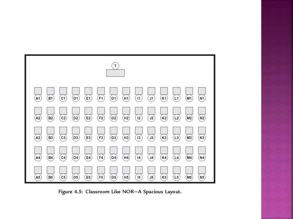
Most memories are designed similarly to the classroom. There are rows and columns, and word lines to tell the memory bits which row is being requested and bit lines to access a column within that row. Figure 4.5

14
Each of the desks :a bit transistor in the memory the students: data Teacher : system interface that handles the data transaction between the rest of the system and the memory bits

15
When a memory bit is requested….. the teacher calling a student to the front of the room. the teacher in this example called for student B3 to come to the front of the room (Figure 4.6). That student would simply walk from his or her desk up the aisle to go to the teacher’s desk. All students could get to the teacher’s desk in about the same amount of time, and it would not take very long to get there.
. That student would simply walk from his or her desk up the aisle to go to the teacher’s desk. All students could get to the teacher’s desk in about the same amount of time, and it would not take very long to get there..")
17
1.All data can be accessed rapidly 2. all accesses take about the same amount of time. 3. Data can be requested from individual locations in a completely random sequence.

18
shrink the size of each classroom which they can do if they push all the desks up against each other, with the desks on one side of the classroom pushed right against the wall. This is illustrated in Figure 4.7

19
when the teacher calls student B3 to the front of the room, all the students in B3’s row must get up and walk to the front of the room in a line (Figure 4.8). There is simply not enough space for them to do it. Once the row is in front, then B3, or C3, or N3, or any of these students can get to the teacher rapidly. On the other hand, none of these students can reach the front of the room until all the students blocking the way have gone to the front.

21
1. many bits in NAND share a bit line,(like the students share a single aisle at the far side of the classroom) 2. reducing the amount of space used on the NAND die to move data back and forth to the bit transistors. 3. NAND takes a longer time to get a memory bit (a student) that is randomly called to the rest of the system (the front of the class). Once that bit line’s data is ready (the student’s row is in the front) then data from that word line can be presented to the system at a 4. rapid-fire rate (just as every student in that row can get to the teacher’s desk very quickly).
 2. reducing the amount of space used on the NAND die to move data back and forth to the bit transistors. 3. NAND takes a longer time to get a memory bit (a student) that is randomly called to the rest of the system (the front of the class). Once that bit line’s data is ready (the student’s row is in the front) then data from that word line can be presented to the system at a 4. rapid-fire rate (just as every student in that row can get to the teacher’s desk very quickly)..")
22
1.NAND less expensive to manufacture than NOR (the manufacturing cost of a silicon chip is a function of its size) 2. Although NOR usually seems easier to use, surprisingly enough, this difference in functionality actually makes NAND a better fit than NOR in applications where serial accesses are preferred to random accesses. * Video and audio streaming are two very good examples of applications where serial access is preferable to random.

24
Flash memory technology : floating gate semiconductor technology & nonvolatile storage* technology That is widely used in mobile consumer electronics applications

25
basic operations of a flash memory ? reading, writing, and erasing. To rewrite data on a fl ash memory ? the flash memory cells must first undergo an erasure step.

26
There are two kinds of flash memory: NOR and NAND. difference the two types of architecture : real estate. NAND has a smaller die size than does NOR. that cause to cost savings. different between NAND and other memory technologies : NAND is partially serial and partially parallel.

27
The serial technology in NAND is very prone to bit errors( Like hard disk drives). designer use error correction technology to correct bit errors. A sector of data will have some parity bits added to check for errors in the sector data.

28
Wear leveling is a technique to spread the writing and erasing over all the cells,so that individual cells do not wear out before the rest of the memory. Wear leveling is managed by the flash memory controller chip.

29
The controller* is also responsible for bad block management in the memory. ( The controller keeps track of the number of bad blocks in each sector, and if the number of bad blocks becomes too large, the sector is declared bad and not used anymore. The data that was on that sector is then moved to a spare unused sector.)
.")
30
Flash memory can be used as a chip installed within the circuit board of a device, or it may be embedded in a removable card. Like a hard disk drive, the flash contains files, and those files must be managed.

31
to increase the storage capacity for a NAND flash memory device with a fixed number of memory cells, the number of bits per cell can be increased.****** ( Implementation of MLC (Multilevel cells) involves more sophisticated controller technology, and this sophistication and processing power has to increase as the number of bits per cell increases).
 involves more sophisticated controller technology, and this sophistication and processing power has to increase as the number of bits per cell increases).")
32
Flash memory dies can be stacked on top of each other to achieve greater volumetric storage capacity.

33
Flash reliability is dependent upon careful control of cell wear and error correction. Flash memory is inherently insensitive to shock or vibration, since it is a solid state storage technology.

34
Removable flash memory card formats have developed over the years due to new applications, form factors, and proprietary designs. the most common fl ash card formats: MMC, SSD, memory card, and miniaturized versions of these formats.

35
flash memory price reduction (expressed in $/GB) should continue at about a 40 percent annual rate for the near future. [With the lower base price for flash memory (compared to other technologies such as hard disk drives) flash memory will be found in lower storage capacity consumer electronics products with growth potential into higher capacity products.]
 flash memory will be found in lower storage capacity consumer electronics products with growth potential into higher capacity products.].")
37
1. Data integrity: accurate data storage & integrity without battery reliance 2. Die size : physical surface area size on the wafer.it is typically measure in square millimeter.

Similar presentations


 Last lecture: –Memory Architecture –Static Ram This lecture –Dynamic Ram –E 2 memory.>")
