Download presentation
Presentation is loading. Please wait.

1
List of Authors: Maria Rita Coluccia, J. A. Appel, G. Chiodini, D. C. Christian, S. W. Kwan, G. Sellberg with Fermi National Accelerator Laboratory L. Uplegger with INFN Milano (Italy)
.")
2
We present IV and CV curves for irradiated prototype n + /n/p + silicon pixel sensors, intended for use in the BTeV experiment at Fermilab. We tested pixel sensors from different vendors and with two pixel isolation techniques: p-stop and p- spray. Results are based on exposure with 200 MeV protons up to 6 x 10 14 protons/cm 2. ABSTRACT

4
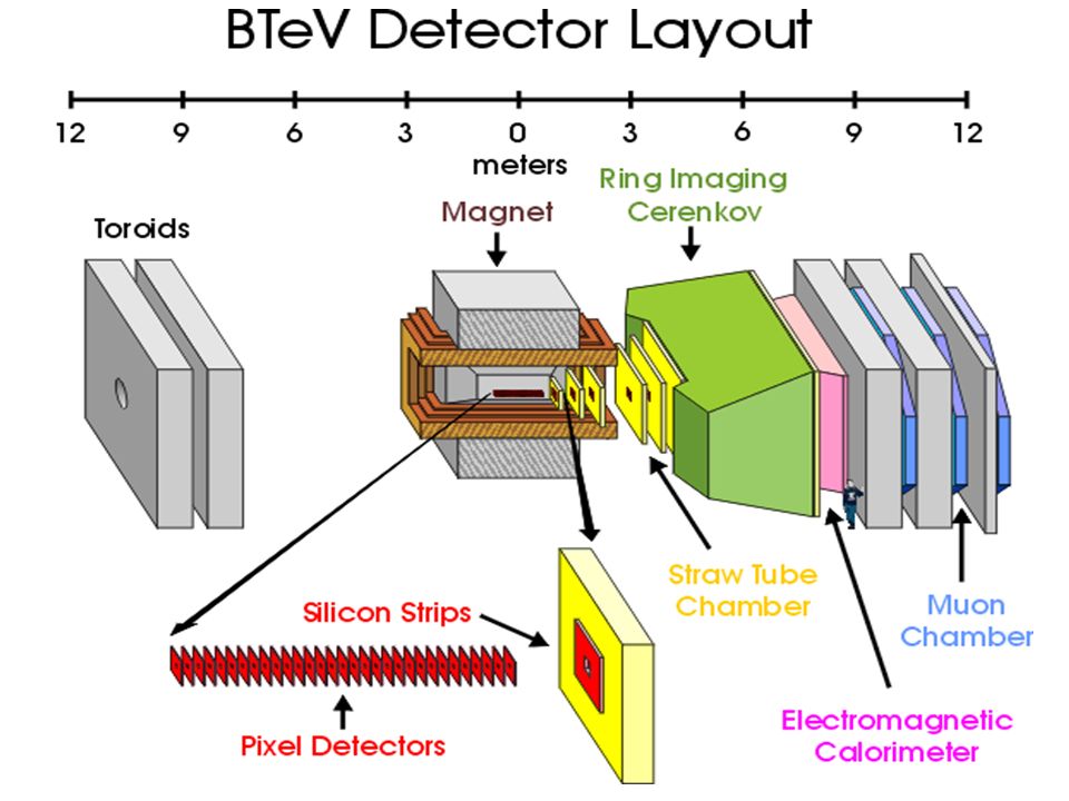
BTeV [1] is a new heavy quark experiment that will run at the TEVATRON collider at Fermi National Accelerator Laboratory. It is designed to cover the “forward” region of the proton-antiproton interaction point running at a luminosity of 2 x 10 32 cm -2 s -1. The experiment will employ a silicon pixel vertex detector to provide high precision space points for an on-line lowest-level trigger based on track impact parameters [2].
![BTeV [1] is a new heavy quark experiment that will run at the TEVATRON collider at Fermi National Accelerator Laboratory.](http://images.slideplayer.com/25/7633210/slides/slide_4.jpg "It is designed to cover the forward region of the proton-antiproton interaction point running at a luminosity of 2 x cm -2 s -1. The experiment will employ a silicon pixel vertex detector to provide high precision space points for an on-line lowest-level trigger based on track impact parameters [2]..")
5
ONE STATION THE VERTEX DETECTOR The baseline BTeV silicon pixel detector has rectangular 50 μm x 400 μm pixel elements and consists of a regular array of 30 “stations” of “planar” pixel detectors distributed along the interaction region.

6
L-SHAPE HALF PLANE Each station contains one plane with the narrow pixel dimension vertical, and one with the narrow dimension horizontal, and is split in order to allow the sensors to be moved away from the beam during acceleration and other unstable beam conditions.

7
HYBRID ASSEMBLY The basic building block of the detector is a hybrid assembly consisting of a sensor, a number of readout chips and a flexible printed circuit (a high-density interconnect: HDI).
.")
8
SENSOR DESIGN The BTeV pixel sensors have n + /n/p + configuration and therefore it is necessary to provide explicit electrical isolation between neighboring n + electrodes. We explore two techniques. P-STOP isolation technique [3] in which a high dose p-implant surrounds each n + -type region. P-STOP ISOLATION TECHNIQUE

9
P-SPRAY ISOLATION TECHNIQUE P-SPRAY isolation technique [4], developed by the ATLAS collaboration, that consists of a medium dose p-implant that is applied to the entire n-side and is overcompensated by the high dose n + pixel implants. To increase radiation hardness and the breakdown voltage before irradiation, a “grading” of p-spray implantation (moderated p- spray) [5] is used, that leads to a step in the effective p-spray dose along the gap between two n + -implants.
![P-SPRAY ISOLATION TECHNIQUE P-SPRAY isolation technique [4], developed by the ATLAS collaboration, that consists of a medium dose p-implant that is applied to the entire n-side and is overcompensated by the high dose n + pixel implants.](http://images.slideplayer.com/25/7633210/slides/slide_9.jpg "To increase radiation hardness and the breakdown voltage before irradiation, a grading of p-spray implantation (moderated p- spray) [5] is used, that leads to a step in the effective p-spray dose along the gap between two n + -implants..")
10
DEVICES TESTED P-STOP sensors From SINTEF (Norway). Low resistivity (1.0-1.5 KΩcm) silicon, 270μm thick. Two arrays tested: 1.test-sized sensors 12 x 92 cells that, except for four, are all connected together. 2.FPIX1-sized sensors 18 x 160 cells (same size as the readout chip FPIX1 [6], no bias grid structure). P-SPRAY sensors From TESLA (Czech Republic) and CiS (Germany). High resistivity (2-5 KΩ cm) silicon, 250 μm thick. One array tested (FPIX1-sized sensors). Bias grid structure for biasing all the pixel simultaneously.
 silicon, 270μm thick. Two arrays tested: 1.test-sized sensors 12 x 92 cells that, except for four, are all connected together. 2.FPIX1-sized sensors 18 x 160 cells (same size as the readout chip FPIX1 [6], no bias grid structure). P-SPRAY sensors From TESLA (Czech Republic) and CiS (Germany). High resistivity (2-5 KΩ cm) silicon, 250 μm thick. One array tested (FPIX1-sized sensors). Bias grid structure for biasing all the pixel simultaneously..")
11
P-STOP SENSOR PERFORMANCES I-V CURVES BEFORE IRRADIATION Fig. 1 Typical I-V curves for both devices before irradiation. The test-sized sensors show very good performance. The FPIX1-sized sensors have lower breakdown voltage. This appears to be related to the fact that it is difficult to bias all of the pixel cells during wafer testing.

12
Fig. 2 The breakdown voltage of the FPIX1-sized sensors increases considerably after bump bonding to a readout chip. We tested 5 sensors that were bump bonded to a readout chip and 3 sensors, with indium bumps deposited on the n + side, that were glued with conductive silver epoxy to a piece of silicon in order to mimic the presence of the readout chip. I-V CURVES BEFORE IRRADIATION

13
I-V CURVES AFTER IRRADIATION Fig. 3 I-V curves for a test-sized p-stop sensor irradiated up to 1.5 E14 p/cm -2 The current after irradiation increases by a few orders of magnitude. However, operating at lower temperature can alleviate this problem.

14
Leakage Current: Temperature Dependence Fig. 4 We repeated the measurements at various temperatures (10 o C, 0 o C and -10 o C). As expected, we observed that the current decreases exponentially with temperature (I leak T 2 exp (-E / 2k B T) [7]). The figure shows the comparison between data and the predicted dependence of the leakage current vs temperature. There is good agreement between the fit and the data.
. As expected, we observed that the current decreases exponentially with temperature (I leak T 2 exp (-E / 2k B T) [7]). The figure shows the comparison between data and the predicted dependence of the leakage current vs temperature. There is good agreement between the fit and the data..")
15
C-V CURVES AND DEPLETION VOLTAGE Fig. 5 Depletion voltage as a function of proton fluence. Note that for 1 year of BTeV running at nominal luminosity the fluence will be 1 x 10 14 p/ cm 2

16
C-V CURVES AND DEPLETION VOLTAGE Fig. 6 Here a typical example of bulk capacitance versus bias potential for a test-sized p-stop irradiated up to 1.2 x 10 14 p/cm 2. We use this method to determine the depletion voltage.

17
P-SPRAY SENSORS PERFORMANCE I-V CURVES BEFORE AND AFTER IRRADIATION Fig. 7 We irradiated two of these sensors, one up to 8 10 13 p/cm 2 and the other one up to 1.2 10 14 p/cm 2. The figure shows the increase in the leakage current due to the irradiation for the most irradiated sensor.

18
C-V CURVE AFTER IRRADIATION Fig. 8 CV measurement for sensor irradiate to 1.2 10 14 p/cm 2. Vdep ~70 V. Before irradiation was Vdep ~60 V. Type inversion already occurred.

19
CONCLUSIONS Two different pixel isolation techniques were studied: P-stop isolation: 1.Most of the tested sensors meet specifications. 2.Problem to measure the breakdown voltage before bump bonding to readout chip. P-spray isolation: 1.Results obtained are promising. 2.It is possible to determine the breakdown voltage due to a bias grid. 3.Need more irradiation studies. We will study the performance of these sensors, bump bonded to a readout chip, in a test beam.

20
REFERENCES [1] A. Kulyavtsev, M. Procario, J. Russ, J. You, J. Cumalat, J. Appel, et al. "BTeV proposal," Fermilab, May 2000. [2] E. E. Gottschalk, "BTeV detached vertex trigger," Fermilab-CONF-01-088- E, June 2001. [3] G. Batagnani, F. Bosi, L. Bosisio, A. Conti, E. Focardi, F. Forti, et al.. "Double-sidedreadout silicon strip detectors for the ALEPH minivertex," Nucle. Instr. Meth., vol. A 277, pp 147-153, 1989. [4] R. H. Richter, L. Andricek, T. Gebhart, D. Hauff, J. Kemmer, G. Lutz, et al., “Strip detector design for ATLAS and HERA-B using two-dimensional device simulation," Nucle. Instr. Meth., vol. A 377, pp 412-421, 1996. [5] G. Lutz, et al., Streifendetektor, Patentoffenlegungsschrift-OS 196 20 081 A1 21.11.97, Munich, 1997 [6] D. C. Christian, et al.. “Development of a pixel readout chip for BTeV,“ Nucle. Instr. Meth., vol. A 335, pp 144, 1999. [7] M. R. Coluccia, et al., “Characterization of prototype BTeV silicon pixel sensors before and after irradiation," accepted for publication in IEEE Trans. Nucl. Sci., Aug. 2002.
![REFERENCES [1] A. Kulyavtsev, M. Procario, J. Russ, J.](http://images.slideplayer.com/25/7633210/slides/slide_20.jpg "You, J. Cumalat, J. Appel, et al. BTeV proposal, Fermilab, May [2] E. E. Gottschalk, BTeV detached vertex trigger, Fermilab-CONF E, June [3] G. Batagnani, F. Bosi, L. Bosisio, A. Conti, E. Focardi, F. Forti, et al.. Double-sidedreadout silicon strip detectors for the ALEPH minivertex, Nucle. Instr. Meth., vol. A 277, pp , [4] R. H. Richter, L. Andricek, T. Gebhart, D. Hauff, J. Kemmer, G. Lutz, et al., Strip detector design for ATLAS and HERA-B using two-dimensional device simulation, Nucle. Instr. Meth., vol. A 377, pp , [5] G. Lutz, et al., Streifendetektor, Patentoffenlegungsschrift-OS A , Munich, 1997 [6] D. C. Christian, et al.. Development of a pixel readout chip for BTeV, Nucle. Instr. Meth., vol. A 335, pp 144, [7] M. R. Coluccia, et al., Characterization of prototype BTeV silicon pixel sensors before and after irradiation, accepted for publication in IEEE Trans. Nucl. Sci., Aug")
Similar presentations


 at Indiana University Cyclotron Facility on 30th November. Pixel 7,44 and.>")


1 MeV eq-n cm -2 02.113.6 *10 13 13.55.7*10 13 25.92.3*10 13 39.11.1*10 13 411.90.7*10 13 514.70.5*10.>")


 The University of Melbourne.>")