Download presentation
Presentation is loading. Please wait.

1
The Sun

2
The Sun Big Bang nucleosynthesis
5 billion years old, 5 billion more years before death Radiated energy determines age Diameter 110 x earth, 99.86% mass of solar system ~90 million miles from earth = 1 AU, ~8 minutes for light ~75% H, 23% He, rest heavy elements, 2% heavy elements Surface temperature ~6,000°C 1.4x10³ kg/m3, 24 x g ,(water 1.0x10³ kg/m3) Nuclear Fusion – 500,000 tons H/sec 100 earths so far Brighter than 85% of stars in Milky Way – Red Dwarfs
 Nuclear Fusion – 500,000 tons H/sec. 100 earths so far. Brighter than 85% of stars in Milky Way – Red Dwarfs.")
4
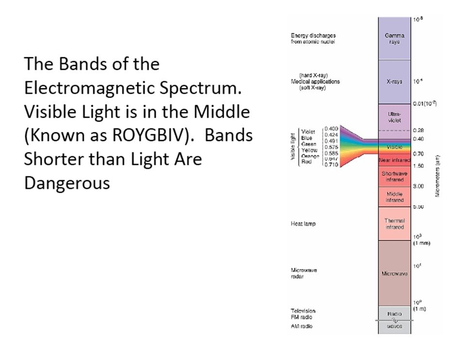
Blackbody Radiation Thermal Radiation Is Electromagnetic Radiation Emitted From A Material Which Is Due To Its Temperature

5
The Sun Magnetically active, 11 year cycle: Sunspots, Solar flares
Solar wind (disruption of communications and electric power) Made of gas and plasma H fusion now, He in 5 billion years Stellar nucleosynthesis
 Made of gas and plasma. H fusion now, He in 5 billion years. Stellar nucleosynthesis.")
6
Sunspots and the Sunspot Cycle

11
Photovoltaics

12
How Much Solar Irradiance Do You Get?
You can get the basic idea of the average irradiance over the United States in W-hrs per square meter per day from this map, which is the average daily solar radiation from It should be noted that this map is meant to give you a feel for solar irradiance. The best data and easiest to use to design a system is available in table/spreadsheet form. For non-tracking arrays, you want the global insolation on a surface tilted at the latitude facing south (for northern hemisphere). Sources:
. Sources:")
13
Solar Cell Land Area Requirements for the World’s Energy with Solar PV
This is the Solar Cell Land Area Requirements. Each box at 3.3 TW. Source: Compliments of Richard Smalley’s lectures on energy 6 Boxes at 3.3 TW Each

14
A Brief History Photovoltaic Technology
– Photovoltaic effect discovered by Becquerel 1870s – Hertz developed solid selenium PV (2%) – Photoelectric effect explained by A. Einstein 1930s – Light meters for photography commonly employed cells of copper oxide or selenium – Bell Laboratories developed the first crystalline silicon cell (4%) – PV cells on the space satellite U.S. Vanguard (better than expected) Here is the timeline of photovoltaic technology. Solar cell technology is actually pretty old. The photovoltaic effect was discovered in the late 1830’s. An explanation of the photoelectric effect won Einstein the Nobel prize. There was a big break through in 1954 because the first crystalline silicon solar cell was developed. Four years later it was used on a space satellite. The good news is that it worked, the bad news is that the solar cells kept working past when NASA expected so then the satellite kept sending data to earth when it was no longer needed and took up E and M bandwidth.
 1905 – Photoelectric effect explained by A. Einstein. 1930s – Light meters for photography commonly employed cells of copper oxide or selenium – Bell Laboratories developed the first crystalline silicon cell (4%) 1958 – PV cells on the space satellite U.S. Vanguard (better than expected) Here is the timeline of photovoltaic technology. Solar cell technology is actually pretty old. The photovoltaic effect was discovered in the late 1830’s. An explanation of the photoelectric effect won Einstein the Nobel prize. There was a big break through in 1954 because the first crystalline silicon solar cell was developed. Four years later it was used on a space satellite. The good news is that it worked, the bad news is that the solar cells kept working past when NASA expected so then the satellite kept sending data to earth when it was no longer needed and took up E and M bandwidth.")
15
Things Start To Get Interesting...
mid 1970s – World energy crisis = millions spent in research and development of cheaper more efficient solar cells 1976 – First amorphous silicon cell developed by Wronski and Carlson 1980’s - Steady progress towards higher efficiency and many new types introduced 1990’s - Large scale production of solar cells more than 10% efficient with the following materials: Ga-As and other III-V’s CuInSe2 and CdTe TiO2 Dye-sensitized Crystalline, Polycrystalline, and Amorphous Silicon Today, prices continue to drop and new “3rd generation” solar cells are researched In the mid 1970’s people were getting worried because of the oil crisis and OPEC. Because people were worried, more thought and money was given to find new and cheaper ways of making solar cells. One development that came out of this research push was the first amorphous silicon cell developed by Chris Wronski and Dave Carlson. The discovery of the amorphous silicon solar cells caused a lot of excitement because it was a fundamentally cheaper material than standard crystalline silicon. This material is also used for the thin film transistors that drive modern flat panel displays. They have been mass produced real cheap, and over the years the price for a flat panel has gone down significantly. The same is happening for solar cell prices. In the 1980’s the solar photovoltaic community made steady progress towards higher efficiency and many new types of solar cells were introduced so that by the 1990’s there were large scale production of solar cells more than 10% efficient with the following materials: Ga-As and other III-V’s, CuInSe2 and CdTe, TiO2 Dye-sensitized, and finally the largest producers Crystalline, Polycrystalline, and Amorphous Silicon solar cells. Today prices continue to drop and new “3rd generation” solar cells are researched.

16
Types of Solar Photovoltaic Materials
This graph show the record efficiency of different types of solar cells as a function of time. What is important to see here is that all the different types of solar cells follow the same trend – as more research is undertaken the efficiencies go up which will drive down the cost of solar electricity relative to fossil fuel fired electricity.

17
Photovoltaic Materials
Solar cells are made from semiconductors - the most important being silicon. Semiconductors have special electronic properties which allow them to be insulating or conducting depending on their composition. In photovoltaic materials you are dealing with the semiconductors (yellow). Most of the doping comes from boron and phosphorous for silcion solar cellsate. There are different types of solar cells such as cadmium telluride (CdTe) made from Cadmium and Tellurium or copper indium diselenide or gallium aresenide. Source:
. Most of the doping comes from boron and phosphorous for silcion solar cellsate. There are different types of solar cells such as cadmium telluride (CdTe) made from Cadmium and Tellurium or copper indium diselenide or gallium aresenide. Source:")
18
Energy Bands in a Semiconductor
Conduction Band – Ec – empty Valence Band – Ev – full of electrons Energy of an electron in a semiconductor must fall between two defined bands. The valence band are energies of valence orbitals which form bonds between atoms. The conduction band, next higher up, is separated from the valence band by and energy gap, or bandgap. The width of the energy gap, Eg, is defined by the difference in energy of the conduction and valence bands: Ec- Ev. This is the energy band structure for a typical semiconductor in detail like silicon. This is your valence band and conduction band. There is an energy gap noted Eg between the two. The valence band is filled with electrons the energy of electrons is going up. A hole is an absence of an electron. The conduction band is empty at absolute zero but at room temperature some valence electrons are excited into it and free to travel. For the remainder of the presentation, if something is full (almost full) the color will be dark and if something is empty (or almost empty) the color will be light. For example, dark green means full valence band and light green means empty conduction band.
 the color will be dark and if something is empty (or almost empty) the color will be light. For example, dark green means full valence band and light green means empty conduction band.")
19
3 Types of Semiconductors
Intrinsic n-type p-type Types 2 and 3 are semiconductors that conduct electricity - How? By alloying semiconductor with an impurity, also known as doping Carriers placed in conduction band or carriers removed from valence band There are three types of semiconductors. There is the intrinsic, which we just discussed (green). There are no extra electrons in conduction band and the valence band is full at absolute zero. Then there is the n-type (orange). It has extra electrons, in the conduction band, which are denoted by the blue circles. The extra electrons pull the Fermi level (black line) up towards the conduction band. For clarity the Fermi energy was not shown for the intrinsic semiconductor – although in this case it would be in the middle of the gap. The p-type (purple) is when you have extra holes in valence band and the Fermi level is closer to the valence band. You can create n and p type semiconductors by placing atoms of a different element inside the lattice. For example, you can place elements in row three and row five (B and P) and remove electrons or give extra ones respectively for silicon.
. There are no extra electrons in conduction band and the valence band is full at absolute zero. Then there is the n-type (orange). It has extra electrons, in the conduction band, which are denoted by the blue circles. The extra electrons pull the Fermi level (black line) up towards the conduction band. For clarity the Fermi energy was not shown for the intrinsic semiconductor – although in this case it would be in the middle of the gap. The p-type (purple) is when you have extra holes in valence band and the Fermi level is closer to the valence band. You can create n and p type semiconductors by placing atoms of a different element inside the lattice. For example, you can place elements in row three and row five (B and P) and remove electrons or give extra ones respectively for silicon.")
20
p-n and p-i-n Junctions
Vbi Vbi Ef Ef Here are the first two types of junctions. The p-n and p-i-n junctions. You have the conduction band and valence band. No electrons can exist in band gap, however, semiconductors are not perfect. In thermodynamic equilibrium at room temperature, you actually populate some of the states in this band gap. The solid line is the Fermi level. You can think of it as electrons as a liquid being poured into a bucket (the gap) and being filled up to the Fermi level. In semiconductors, when you put two dissimilar semiconductors together, the Fermi level must stay flat. This is what created the bending of these bands (both the conduction and valence band). So in the p-n junction you have the p layer and an n layer. In the p-type the Fermi level is very low in the gap an pulled to the valence band. In the n-type semiconductor, the Fermi level is very high and pulled toward the conduction band. There is an enormous bending of the conduction and valence bands due to trying to keep Fermi level flat when they are combined. The bending creates the voltage and the electric field observed when putting two dissimilar (p and n) semiconductors together. The energy between the conduction band in the p-layer and the n-layer is the built in potential. What happens when you put an intrinsic layer of semiconductor between the p and n types? Well now, this bending of the bands is spaced out. The Fermi level still flat.
 and being filled up to the Fermi level. In semiconductors, when you put two dissimilar semiconductors together, the Fermi level must stay flat. This is what created the bending of these bands (both the conduction and valence band). So in the p-n junction you have the p layer and an n layer. In the p-type the Fermi level is very low in the gap an pulled to the valence band. In the n-type semiconductor, the Fermi level is very high and pulled toward the conduction band. There is an enormous bending of the conduction and valence bands due to trying to keep Fermi level flat when they are combined. The bending creates the voltage and the electric field observed when putting two dissimilar (p and n) semiconductors together. The energy between the conduction band in the p-layer and the n-layer is the built in potential. What happens when you put an intrinsic layer of semiconductor between the p and n types Well now, this bending of the bands is spaced out. The Fermi level still flat.")
21
Schottky Barriers and Heterojunctions
A Schottky barrier is a potential barrier formed at a metal–semiconductor junction which has rectifying characteristics, suitable for use as a diode The largest differences between a Schottky barrier and a p–n junction are its typically lower junction voltage, and decreased (almost nonexistent) depletion width in the metal Here are the next two types of junctions that can be used for solar cells: Schottcky Barriers and Heterojunctions. For the Schottcky barrier, there is a metal, filled with electrons, placed right beside the semiconductor. This creates the bend in the band. This type of junction is a way to test semiconductors and is generally not technically practical for solar cells in production. The heterojunction has two different semiconductors put together that have different energies. When these two semiconductors are put together, they create a bend in the band as well.
 depletion width in the metal. Here are the next two types of junctions that can be used for solar cells: Schottcky Barriers and Heterojunctions. For the Schottcky barrier, there is a metal, filled with electrons, placed right beside the semiconductor. This creates the bend in the band. This type of junction is a way to test semiconductors and is generally not technically practical for solar cells in production. The heterojunction has two different semiconductors put together that have different energies. When these two semiconductors are put together, they create a bend in the band as well.")
22
I-V Curve for Solar Cells
This is the same graph as before only flipped around to highlight the 4th quadrant of the I-V plot (Current density vs. Voltage). As V=0, you have maximum current, which is called the short circuit current. If you increase voltage, the current decreases. If you continue to increase voltage, the current goes to zero, and this is called an open circuit. The dashed line signifies power density and is shown on the right axis. The maximum current density and voltage is at the maximum power point, because after that, the power drops off, as well as the current. Maximum power for current= Jmp. Maximum power for voltage= Vmp. Fill factor is defined as: FF= (Imax)( Vmax) / short circuit open circuit. A 100% fill factor would have a square angle in the figure.
. As V=0, you have maximum current, which is called the short circuit current. If you increase voltage, the current decreases. If you continue to increase voltage, the current goes to zero, and this is called an open circuit. The dashed line signifies power density and is shown on the right axis. The maximum current density and voltage is at the maximum power point, because after that, the power drops off, as well as the current. Maximum power for current= Jmp. Maximum power for voltage= Vmp. Fill factor is defined as: FF= (Imax)( Vmax) / short circuit open circuit. A 100% fill factor would have a square angle in the figure.")
23
Light Absorption by a Semiconductor
Photovoltaic energy relies on light Light → stream of photons → carries energy Example: On a clear day 4.4x10¹⁷ photons hit 1 m2 of Earth’s surface every second. Eph()=hc/ h = plank’s constant = x J-s = wavelength c = speed of light =3 x 10⁸ m/s f = frequency However, only photons with energy in excess of bandgap can be converted into electricity by solar cells In order for a solar cell to work, it has to absorb light. Light is basically a stream of photons, which are quantized packets of light energy. There is a huge amount of photons in light. For example, on a clear day 4.4x10¹⁷ photons hit 1 m2 of Earth’s surface every second. Each photon has energy associated with it that depends on the wavelength, or the color of the light. This is shown in the Energy equation for a photon: Eph()=hc/=hf, where h = plank’s constant = x J-s, = wavelength, c = speed of light =3 x 10⁸ m/s, and f = frequency. However, only photons with energy in excess of bandgap energy can be converted into electricity by solar cells. This is because, when light shines on a semiconductor the only photons that are absorbed have at least the energy of the bandgap. Photons that are too small will not be absorbed and will go straight through the band gap. So, in general, photons need to have enough energy to excite an electron from the valence band up to the conduction band.
=hc/ h = plank’s constant = x J-s. = wavelength. c = speed of light =3 x 10⁸ m/s. f = frequency. However, only photons with energy in excess of bandgap can be converted into electricity by solar cells. In order for a solar cell to work, it has to absorb light. Light is basically a stream of photons, which are quantized packets of light energy. There is a huge amount of photons in light. For example, on a clear day 4.4x10¹⁷ photons hit 1 m2 of Earth’s surface every second. Each photon has energy associated with it that depends on the wavelength, or the color of the light. This is shown in the Energy equation for a photon: Eph()=hc/=hf, where h = plank’s constant = x J-s, = wavelength, c = speed of light =3 x 10⁸ m/s, and f = frequency. However, only photons with energy in excess of bandgap energy can be converted into electricity by solar cells. This is because, when light shines on a semiconductor the only photons that are absorbed have at least the energy of the bandgap. Photons that are too small will not be absorbed and will go straight through the band gap. So, in general, photons need to have enough energy to excite an electron from the valence band up to the conduction band.")
24
The Solar Spectrum The entire spectrum is not available to single junction solar cell This is the Solar Spectrum. The graph shows the flux of photons that come down to the Earth vs. the wavelength of the photons. The Orange line represents the solar spectrum outside the atmosphere. The spectrum reaches a peak in the visible as expected from black body radiation at 5800K (the surface temperature of the sun). The missing regions of flux (black line) at the earth’s surface are due to absorption from water vapor and carbon dioxide. As you can clearly see, the solar energy is not just a single energy (wavelength or frequency of light). If it were, we would have solar cells based on current technology with efficiencies over 95%. So why do we lose energy at different wavelengths? Part of it is because we are not absorbing the whole spectrum of a single photon. If we put in photons with larger energies than the bandgap we only capture the energy equal to Eg – we lose the rest to waste heat. Photons with energies lower than the bandgap do not contribute to carriers (electrons and holes) in a solar cell. Source:
. The missing regions of flux (black line) at the earth’s surface are due to absorption from water vapor and carbon dioxide. As you can clearly see, the solar energy is not just a single energy (wavelength or frequency of light). If it were, we would have solar cells based on current technology with efficiencies over 95%. So why do we lose energy at different wavelengths Part of it is because we are not absorbing the whole spectrum of a single photon. If we put in photons with larger energies than the bandgap we only capture the energy equal to Eg – we lose the rest to waste heat. Photons with energies lower than the bandgap do not contribute to carriers (electrons and holes) in a solar cell. Source:")
25
Generation of Electron Hole Pairs with Light
Photon enters, is absorbed, and lets electron from VB get sent up to CB Therefore a hole is left behind in VB, creating absorption process: electron-hole pairs Because of this, only part of solar spectrum can be converted The photon flux converted by a solar cell is about 2/3 of total flux So what happens to a photon that is absorbed in a semiconductor? The photon enters and is absorbed and thereby excites an electron from the valence band up to the conduction band. The extra energy of the photon is then lost and turned into heat. Because of that, only 2/3 of the total flux can be turned into electricity. Even after that, more energy flux can be lost from thermal process.

26
Electron Flow in a PV Cell

27
Generation Current Generation Current = light induced electrons across bandgap as electron current Electron current:= Ip=qNA N = # of photons in highlighted area of spectrum A = surface area of semiconductor that’s exposed to light Because there is current from light, voltage can also occur Electric power can occur by separating the electrons and holes to the terminals of device Electrostatic energy of charges occurs after separation only if its energy is less than the energy of the electron-hole pair in semiconductor Therefore, Vmax=Eg/q Vmax= bandgap of semiconductor is in EV’s, therefore this equation shows that wide bandgap semiconductors produce higher voltage When a photon is absorbed it generates current. Generation current is just light induced electrons across the band gap as electron current. The equation for electron current is Ip=qNA. Where q is the charge, N is the number of photons in the highlighted area of the spectrum and A is the surface area of semiconductor that’s exposed to light. Because the of this the maximum Voltage it will ever get to is just the band gap energy in electron-volts, or eV’s. Electrostatic energy of charges occurs after separation only if its energy is less than the energy of the electron-hole pair in semiconductor. Therefore Vmax=Eg/q, where q is the charge on an electron – if Eg is measured in electron –volts eV, you are left with voltage. Vmax= bandgap of semiconductor is in EV’s, therefore this equation shows that wide bandgap semiconductors produce higher voltage.

28
Different Types of Photovoltaic Solar Cells
Diffusion Drift Excitonic There are three different types of solar cells. The most established is diffusion. The other two are drift and excitonic and represent 2nd and 3rd generation types of solar cells, respectively.

29
Diffusion n-type and p-type are aligned by the Fermi-level
When a photon comes in n-type, it takes the place of a hole, the hole acts like an air bubble and “floats” up to the p-type When the photon comes to the p-type, it takes place of an electron, the electron acts like a steel ball and “rolls” down to the n-type In diffusion-based silicon solar cell there is the p-n junction. Light is absorbed and excites electrons up to the conduction band. You can think of the electrons in the conduction band as little balls rolling down a hill. So once the electron is excited up to the conduction band, it rolls down the hill. The holes are like air bubbles, they float up inside the valence band. The movement of electrons and holes creates a current. Take note that the direction the current is moving is the opposite of the direction the electrons are moving. This diagram is an example of diffusion. For an electron to “get to the hill” to fall down, it has to diffuse. You have to have a very good crystal for this to work. If not, the defects in the crystal will cause the electrons to combine with the holes and mutually annihilate.

30
Power Losses in Solar Cells
There are physical constraints that create power losses in real solar cells. This diagram shows these constraints. For 100mW of power coming from the sun are coming in, 21 mW is the below the band gap, so its not enough energy to excite an electron. 31mW of it is excess of the band gap so its lost through heat. So already, more than half of your power is lost just because of the limitations of a single bandgap. The Voc available in silicon is 1.1V and because of all the above losses, all you have left are 44 mAmps. Recombination losses, which are electrons smashing into holes, drops the 1.1V to approximately 0.6V. As you can see, recombination cuts the maximum voltage almost in half. Now the current, already being cut down earlier, will be cut down once again due to collection efficiency and incomplete absorption. Collection efficiency is when some of the photons cannot excite electron-hole pairs. Incomplete absorption means some of the photons pass through the cell. This demonstrates one of the technical challenges of designing solar cells: If you make your cell thicker, its easier to absorb photons but harder to collect electrons because they have to diffuse over longer distances. However, if you make the solar cell thinner, it would be easier to collect electrons but you will lose a lot of photons that do not absorb. In addition, there is top surface reflection on a cell and no absorption where the metal is located due to shadowing. The current of 44milliAmps is now decreased to 21 milliAmps. The fill factor is reduced from 1 to .7. The final power is about 14 mW, which means this solar cell is 14% efficient.

31
Recombination Opposite of carrier generation, where electron-hole pair is annihilated Most common at: impurities defects of crystal structure surface of semiconductor Reducing both voltage and current Now we will go through each one of these losses in detail. Recombination is when an electron-hole pair is created and then is smashed back into each other. Recombination usually happens when there is an impurity. For example, if you have a perfect silicon lattice except for the addition of a few sodium atoms. The sodium atoms create defects in the gap which means you end up with nothing instead of an electron-hole pair. There can also be defects in the crystal structure. No matter how perfect the bulk material is, on the surface of a semiconductor there are silicon atoms that are not fully bonded – which then cause surface states. The more surface states you have on the silicon solar cell, such as is created at grain boundaries in a polycrystalline silicon solar cell, the worse off you are. This explains why polycrystalline silicon solar cells do not have as high efficiencies as seen for single crystal silicon solar cells.

32
Stainless Steel Substrate
Tandem Cells Silver Grid Tandem cell- several cells, Top cell has large bandgap Middle cell mid eV bandgap Bottom cell small bandgap Indium Tin Oxide p-a-Si:H Blue Cell i-a-Si:H n-a-Si:H p Green Cell i-a-SiGe:H (~15%) n Red Cell i-a-SiGe:H (~50%) Textured Zinc Oxide Silver Stainless Steel Substrate Another method to increase the efficiencies of solar cells is to use the tandem concept pictured here. This is where several cells are stacked on top of each other. In the example here of a triple junction amorphous silicon solar cell. In order to fabricate a tandem cell you do the following. First, you have stainless steel substrate covered with silver as a back reflector on the bottom. Here when light comes into the cell it is reflected and goes back through for another chance at absorption. Also the back is textured so that the light will scatter and must take a longer path through the material. Next is the red cell (which absorbs red light). It is an p-i-n structure. On top of that is green and then blue cells, which each absorb their respective color of light. Both of those also have the p-i-n structure. Finally, the top surface is made up of a textured transparent conductive layer. The green and red cells are actually silicon germanium. Germanium has a smaller band gap than silicon, so that when you combine those, you get a small gap, then bigger, and bigger, increasing on the way up. The blue cell is on top of the red because blue has a larger band gap it will absorb the highest energy photons and let the photons with less energy (green and red) pass through it to be absorbed by the lower cells. If the tandem cell was turned upside down, the green and blue energy of the photon would get lost because red has the smallest band gap and would absorb them but lose a large percentage of the energy to waste heat. Schematic diagram of state-of-the-art a-Si:H based substrate n-i-p triple junction cell structure
 n. Red Cell. i-a-SiGe:H (~50%) Textured Zinc Oxide. Silver. Stainless Steel Substrate. Another method to increase the efficiencies of solar cells is to use the tandem concept pictured here. This is where several cells are stacked on top of each other. In the example here of a triple junction amorphous silicon solar cell. In order to fabricate a tandem cell you do the following. First, you have stainless steel substrate covered with silver as a back reflector on the bottom. Here when light comes into the cell it is reflected and goes back through for another chance at absorption. Also the back is textured so that the light will scatter and must take a longer path through the material. Next is the red cell (which absorbs red light). It is an p-i-n structure. On top of that is green and then blue cells, which each absorb their respective color of light. Both of those also have the p-i-n structure. Finally, the top surface is made up of a textured transparent conductive layer. The green and red cells are actually silicon germanium. Germanium has a smaller band gap than silicon, so that when you combine those, you get a small gap, then bigger, and bigger, increasing on the way up. The blue cell is on top of the red because blue has a larger band gap it will absorb the highest energy photons and let the photons with less energy (green and red) pass through it to be absorbed by the lower cells. If the tandem cell was turned upside down, the green and blue energy of the photon would get lost because red has the smallest band gap and would absorb them but lose a large percentage of the energy to waste heat. Schematic diagram of state-of-the-art a-Si:H based substrate n-i-p triple junction cell structure.")
Similar presentations


 junctions>")


![Jordan University of Science and Technology Department of applied Physics Solar cells [Operation principles and testing] Advisor: Dr. Adnan Shariah Ghassan.](/16/5222571/big_thumb.jpg "Jordan University of Science and Technology Department of applied Physics Solar cells [Operation principles and testing] Advisor: Dr. Adnan Shariah Ghassan.>")
