Download presentation
Presentation is loading. Please wait.

1
By Squadron Leader Zahid Mir CS&IT Department, Superior University PHY-BE -18 DC Load Line

3
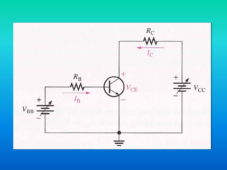
Collector Characteristic Curve Saturation Region Let V BB is set to produce a certain value of I B and V CC is zero. For this condition, both the base- emitter junction and the base- collector junction are forward- biased. – Reason The base is at approximately 0.7V while the emitter and collector are at 0V. The base current is through the base-emitter junction because of low impedance path to grounded, therefore I C is zero. When both junctions are forward- biased, the transistor is said to be in saturation region of its operation.

4
Collector Characteristic Curve Saturation Region As V CC is increased, V CE increases gradually as the collector current increases. This is indicated by the portion of the characteristic curve between A and B. I C increases as V CC is increased because V CE remains less than 0.7V due to the forward-biased base- collector junction.

5
Collector Characteristic Curve Linear Region When V CE exceeds 0.7V, the base-collector junction becomes reverse-biased and the transistor goes into the active or linear region of its operation. Once the base-collector junction is reverse- biased, I C levels off and remains constant for a given value of I B as V CE continues to increase. This is shown by the portion of the characteristic curve between points B and C. When V CE reaches a sufficiently high voltage, the reverse-biased base-collector junction goes into breakdown; and the collector current increases rapidly as indicated by the part of the curve to the right of point C.

6
Collector Characteristic Curve Cutoff Region A small amount of collector current (due to thermally generated electron- hole pairs) flows even when I B =0,it is called I CEO. Since main collector current is zero, the transistor is said to be cut-off. Since I CEO is extremely small, it will usually be neglected in circuit analysis so that V CE = V CC. In cutoff, both the base-emitter and the base-collector junctions are reverse-biased.

7
Collector Characteristic Curve Saturation State When the base-emitter junction becomes forward-biased and the base current is increased, the collector current also increases (I C = βI B ). But V CE decreases due to more drop across collector resistance (V CE = V CC – I C R C ). When V CE reaches its saturation value, V CE(sat), the base-collector junction becomes forward- biased and I C can increase no further even with a continued increase in I B. So at the point of saturation the relation I C = βI B is no longer valid. V CE(sat) for a transistor occurs somewhere below the knee of the collector curves.
. When V CE reaches its saturation value, V CE(sat), the base-collector junction becomes forward- biased and I C can increase no further even with a continued increase in I B. So at the point of saturation the relation I C = βI B is no longer valid. V CE(sat) for a transistor occurs somewhere below the knee of the collector curves..")
8
DC Load Line The voltage equation of a collector-emitter circuit is; V CC = I C R C + V CE I C = V CC /R C - V CE /R C When I C = 0, V CE = V CC ( Cutoff point ) When V CE = 0, I C = V CC /R C ( Saturation point) DC load line is a straight line joining the cutoff and saturation points.
 When V CE = 0, I C = V CC /R C ( Saturation point) DC load line is a straight line joining the cutoff and saturation points.")
9
Active Region of a Transistor All operating points between cutoff and saturation (C,D,E) form the active region of the transistor. In this region emitter-base junction is forward biased and collector-base junction is reversed biased. C

Similar presentations


 NPNPNP.>")


>")


>")


>")
