Download presentation
Presentation is loading. Please wait.

1
Crystallography and Structure ME 2105 R. R. Lindeke

2
Overview: Crystal Structure – matter assumes a periodic shape Non-Crystalline or Amorphous “structures” no long range periodic shapes FCC, BCC and HCP – common for metals Xtal Systems – not structures but potentials Point, Direction and Planer ID’ing in Xtals X-Ray Diffraction and Xtal Structure

3
Non dense, random packing Dense, ordered packing Dense, ordered packed structures tend to have lower energies. Energy and Packing Energy r typical neighbor bond length typical neighbor bond energy Energy r typical neighbor bond length typical neighbor bond energy

4
Crystal Structure Means: PERIODIC ARRANGEMENT OF ATOMS/IONS OVER LARGE ATOMIC DISTANCES Leads to structure displaying LONG-RANGE ORDER that is Measurable and Quantifiable All metals, many ceramics, some polymers exhibit this “High Bond Energy” – More Closely Packed Structure CRYSTAL STRUCTURES

5
Amorphous Materials These less densely packed lower bond energy “structures” can be found in Metal are observed in Ceramic GLASS and many “plastics” Materials Lacking Long range order

6
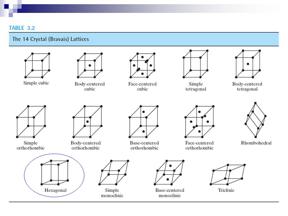
Crystal Systems – Some Definitional information 7 crystal systems of varying symmetry are known These systems are built by changing the lattice parameters: a, b, and c are the edge lengths , , and are interaxial angles Fig. 3.4, Callister 7e. Unit cell: smallest repetitive volume which contains the complete lattice pattern of a crystal.

7
Crystal Systems Crystal structures are divided into groups according to unit cell geometry (symmetry).
.")
9
Tend to be densely packed. Reasons for dense packing: - Typically, only one element is present, so all atomic radii are the same. - Metallic bonding is not directional. - Nearest neighbor distances tend to be small in order to lower bond energy. - Electron cloud shields cores from each other Have the simplest crystal structures. We will examine three such structures (those of engineering importance) called: FCC, BCC and HCP – with a nod to Simple Cubic Metallic Crystal Structures
 called: FCC, BCC and HCP – with a nod to Simple Cubic Metallic Crystal Structures.")
10
Crystal Structure of Metals – of engineering interest

11
Rare due to low packing density (only Po – Polonium -- has this structure) Close-packed directions are cube edges. Coordination No. = 6 (# nearest neighbors) for each atom as seen (Courtesy P.M. Anderson) Simple Cubic Structure (SC)
 for each atom as seen (Courtesy P.M. Anderson) Simple Cubic Structure (SC).")
12
APF for a simple cubic structure = 0.52 APF = a 3 4 3 (0.5a) 3 1 atoms unit cell atom volume unit cell volume Atomic Packing Factor (APF) APF = Volume of atoms in unit cell* Volume of unit cell *assume hard spheres Adapted from Fig. 3.23, Callister 7e. close-packed directions a R=0.5a contains (8 x 1/8) = 1atom/unit cell Here: a = R at *2 Where R at is the ‘handbook’ atomic radius
 = 1atom/unit cell Here: a = R at *2 Where R at is the ‘handbook’ atomic radius.")
13
Coordination # = 8 Adapted from Fig. 3.2, Callister 7e. (Courtesy P.M. Anderson) Atoms touch each other along cube diagonals. --Note: All atoms are identical; the center atom is shaded differently only for ease of viewing. Body Centered Cubic Structure (BCC) ex: Cr, W, Fe ( ), Tantalum, Molybdenum 2 atoms/unit cell: (1 center) + (8 corners x 1/8)
 Atoms touch each other along cube diagonals. --Note: All atoms are identical; the center atom is shaded differently only for ease of viewing. Body Centered Cubic Structure (BCC) ex: Cr, W, Fe ( ), Tantalum, Molybdenum 2 atoms/unit cell: (1 center) + (8 corners x 1/8).")
14
Atomic Packing Factor: BCC a APF = 4 3 (3a/4) 3 2 atoms unit cell atom volume a 3 unit cell volume length = 4R = Close-packed directions: 3 a APF for a body-centered cubic structure = 0.68 a R Adapted from Fig. 3.2(a), Callister 7e. a 2 a 3
, Callister 7e. a 2 a 3.")
15
Coordination # = 12 Adapted from Fig. 3.1, Callister 7e. (Courtesy P.M. Anderson) Atoms touch each other along face diagonals. --Note: All atoms are identical; the face-centered atoms are shaded differently only for ease of viewing. Face Centered Cubic Structure (FCC) ex: Al, Cu, Au, Pb, Ni, Pt, Ag 4 atoms/unit cell: (6 face x ½) + (8 corners x 1/8)
 Atoms touch each other along face diagonals. --Note: All atoms are identical; the face-centered atoms are shaded differently only for ease of viewing. Face Centered Cubic Structure (FCC) ex: Al, Cu, Au, Pb, Ni, Pt, Ag 4 atoms/unit cell: (6 face x ½) + (8 corners x 1/8).")
16
APF for a face-centered cubic structure = 0.74 Atomic Packing Factor: FCC The maximum achievable APF! APF = 4 3 (2a/4) 3 4 atoms unit cell atom volume a 3 unit cell volume Close-packed directions: length = 4R = 2 a Unit cell contains: 6 x 1/2 + 8 x 1/8 =4 atoms/unit cell a 2 a Adapted from Fig. 3.1(a), Callister 7e. (a = 2 2*R)
 3 4 atoms unit cell atom volume a 3 unit cell volume Close-packed directions: length = 4R = 2 a Unit cell contains: 6 x 1/2 + 8 x 1/8 =4 atoms/unit cell a 2 a Adapted from Fig. 3.1(a), Callister 7e. (a = 2 2*R).")
17
Coordination # = 12 ABAB... Stacking Sequence APF = 0.74 3D Projection 2D Projection Adapted from Fig. 3.3(a), Callister 7e. Hexagonal Close-Packed Structure (HCP) 6 atoms/unit cell ex: Cd, Mg, Ti, Zn c/a = 1.633 (ideal) c a A sites B sites A sites Bottom layer Middle layer Top layer
, Callister 7e. Hexagonal Close-Packed Structure (HCP) 6 atoms/unit cell ex: Cd, Mg, Ti, Zn c/a = (ideal) c a A sites B sites A sites Bottom layer Middle layer Top layer.")
18
We find that both FCC & HCP are highest density packing schemes (APF =.74) – this illustration shows their differences as the closest packed planes are “built-up”
 – this illustration shows their differences as the closest packed planes are built-up")
19
Theoretical Density, where n = number of atoms/unit cell A = atomic weight V C = Volume of unit cell = a 3 for cubic N A = Avogadro’s number = 6.023 x 10 23 atoms/mol Density = = VC NAVC NA n An A = Cell Unit of VolumeTotal Cell Unit in Atomsof Mass

20
Ex: Cr (BCC) A = 52.00 g/mol R = 0.125 nm n = 2 a = 4R/ 3 = 0.2887 nm a R = a 3 52.002 atoms unit cell mol g unit cell volume atoms mol 6.023 x 10 23 Theoretical Density, theoretical actual = 7.18 g/cm 3 = 7.19 g/cm 3
 A = g/mol R = nm n = 2 a = 4R/ 3 = nm a R = a atoms unit cell mol g unit cell volume atoms mol x Theoretical Density, theoretical actual = 7.18 g/cm 3 = 7.19 g/cm 3")
21
LOOKING AT THE CERAMIC UNIT CELLS Adding Ionic Complexities

22
Cesium chloride (CsCl) unit cell showing (a) ion positions and the two ions per lattice point and (b) full-size ions. Note that the Cs + −Cl − pair associated with a given lattice point is not a molecule because the ionic bonding is nondirectional and because a given Cs + is equally bonded to eight adjacent Cl −, and vice versa. [Part (b) courtesy of Accelrys, Inc.]
 courtesy of Accelrys, Inc.].")
23
Sodium chloride (NaCl) structure showing (a) ion positions in a unit cell, (b) full-size ions, and (c) many adjacent unit cells. [Parts (b) and (c) courtesy of Accelrys, Inc.]
 and (c) courtesy of Accelrys, Inc.].")
24
Fluorite (CaF 2 ) unit cell showing (a) ion positions and (b) full-size ions. [Part (b) courtesy of Accelrys, Inc.]
 courtesy of Accelrys, Inc.].")
27
Polymorphism: Also in Metals Two or more distinct crystal structures for the same material (allotropy/polymorphism) titanium (HCP), (BCC)-Ti carbon: diamond, graphite BCC FCC BCC 1538ºC 1394ºC 912ºC - Fe - Fe - Fe liquid iron system:
 titanium (HCP), (BCC)-Ti carbon: diamond, graphite BCC FCC BCC 1538ºC 1394ºC 912ºC - Fe - Fe - Fe liquid iron system:")
28
The corundum (Al 2 O 3 ) unit cell is shown superimposed on the repeated stacking of layers of close-packed O 2− ions. The Al 3+ ions fill two-thirds of the small (octahedral) interstices between adjacent layers.
 interstices between adjacent layers..")
29
Exploded view of the kaolinite unit cell, 2(OH) 4 Al 2 Si 2 O 5. (From F. H. Norton, Elements of Ceramics, 2nd ed., Addison-Wesley Publishing Co., Inc., Reading, MA, 1974.)
.")
30
Transmission electron micrograph of the structure of clay platelets. This microscopic-scale structure is a manifestation of the layered crystal structure shown in the previous slide. (Courtesy of I. A. Aksay.)
.")
31
( a) An exploded view of the graphite (C) unit cell. (From F. H. Norton, Elements of Ceramics, 2nd ed., Addison-Wesley Publishing Co., Inc., Reading, MA, 1974.) (b) A schematic of the nature of graphite’s layered structure. (From W. D. Kingery, H. K. Bowen, and D. R. Uhlmann, Introduction to Ceramics, 2nd ed., John Wiley & Sons, Inc., NY, 1976.)
 (b) A schematic of the nature of graphite’s layered structure. (From W. D. Kingery, H. K. Bowen, and D. R. Uhlmann, Introduction to Ceramics, 2nd ed., John Wiley & Sons, Inc., NY, 1976.).")
32
(a) C 60 molecule, or buckyball. (b) Cylindrical array of hexagonal rings of carbon atoms, or buckytube. (Courtesy of Accelrys, Inc.)
 Cylindrical array of hexagonal rings of carbon atoms, or buckytube. (Courtesy of Accelrys, Inc.).")
33
Arrangement of polymeric chains in the unit cell of polyethylene. The dark spheres are carbon atoms, and the light spheres are hydrogen atoms. The unit-cell dimensions are 0.255 nm × 0.494 nm × 0.741 nm. (Courtesy of Accelrys, Inc.)
.")
34
Weaving-like pattern of folded polymeric chains that occurs in thin crystal platelets of polyethylene. (From D. J. Williams, Polymer Science and Engineering, Prentice Hall, Inc., Englewood Cliffs, NJ, 1971.)
.")
35
Diamond cubic unit cell showing (a) atom positions. There are two atoms per lattice point (note the outlined example). Each atom is tetrahedrally coordinated. (b) The actual packing of full-size atoms associated with the unit cell. [Part (b) courtesy of Accelrys, Inc.]
. Each atom is tetrahedrally coordinated. (b) The actual packing of full-size atoms associated with the unit cell. [Part (b) courtesy of Accelrys, Inc.].")
36
Zinc blende (ZnS) unit cell showing (a) ion positions. There are two ions per lattice point (note the outlined example). Compare this structure with the diamond cubic structure (Figure 3.20a). (b) The actual packing of full-size ions associated with the unit cell. [Part (b) courtesy of Accelrys, Inc.]
. Compare this structure with the diamond cubic structure (Figure 3.20a). (b) The actual packing of full-size ions associated with the unit cell. [Part (b) courtesy of Accelrys, Inc.].")
37
Densities of Material Classes metals > ceramics > polymers Why? Data from Table B1, Callister 7e. (g/cm ) 3 Graphite/ Ceramics/ Semicond Metals/ Alloys Composites/ fibers Polymers 1 2 20 30 *GFRE, CFRE, & AFRE are Glass, Carbon, & Aramid Fiber-Reinforced Epoxy composites (values based on 60% volume fraction of aligned fibers in an epoxy matrix). 10 3 4 5 0.3 0.4 0.5 Magnesium Aluminum Steels Titanium Cu,Ni Tin, Zinc Silver, Mo Tantalum Gold, W Platinum Graphite Silicon Glass-soda Concrete Si nitride Diamond Al oxide Zirconia HDPE, PS PP, LDPE PC PTFE PET PVC Silicone Wood AFRE* CFRE* GFRE* Glass fibers Carbonfibers Aramid fibers Metals have... close-packing (metallic bonding) often large atomic masses Ceramics have... less dense packing often lighter elements Polymers have... low packing density (often amorphous) lighter elements (C,H,O) Composites have... intermediate values In general
 3 Graphite/ Ceramics/ Semicond Metals/ Alloys Composites/ fibers Polymers *GFRE, CFRE, & AFRE are Glass, Carbon, & Aramid Fiber-Reinforced Epoxy composites (values based on 60% volume fraction of aligned fibers in an epoxy matrix) Magnesium Aluminum Steels Titanium Cu,Ni Tin, Zinc Silver, Mo Tantalum Gold, W Platinum Graphite Silicon Glass-soda Concrete Si nitride Diamond Al oxide Zirconia HDPE, PS PP, LDPE PC PTFE PET PVC Silicone Wood AFRE* CFRE* GFRE* Glass fibers Carbonfibers Aramid fibers Metals have... close-packing (metallic bonding) often large atomic masses Ceramics have... less dense packing often lighter elements Polymers have... low packing density (often amorphous) lighter elements (C,H,O) Composites have... intermediate values In general.")
38
Some engineering applications require single crystals: Properties of crystalline materials often related to crystal structure. (Courtesy P.M. Anderson) --Ex: Quartz fractures more easily along some crystal planes than others. --diamond single crystals for abrasives --turbine blades Fig. 8.33(c), Callister 7e. (Fig. 8.33(c) courtesy of Pratt and Whitney). (Courtesy Martin Deakins, GE Superabrasives, Worthington, OH. Used with permission.) Crystals as Building Blocks
 --Ex: Quartz fractures more easily along some crystal planes than others. --diamond single crystals for abrasives --turbine blades Fig. 8.33(c), Callister 7e. (Fig. 8.33(c) courtesy of Pratt and Whitney). (Courtesy Martin Deakins, GE Superabrasives, Worthington, OH. Used with permission.) Crystals as Building Blocks.")
39
Most engineering materials are polycrystals. Nb-Hf-W plate with an electron beam weld. Each "grain" is a single crystal. If grains are randomly oriented, overall component properties are not directional. Grain sizes typ. range from 1 nm to 2 cm (i.e., from a few to millions of atomic layers). Adapted from Fig. K, color inset pages of Callister 5e. (Fig. K is courtesy of Paul E. Danielson, Teledyne Wah Chang Albany) 1 mm Polycrystals Isotropic Anisotropic
. Adapted from Fig. K, color inset pages of Callister 5e. (Fig. K is courtesy of Paul E. Danielson, Teledyne Wah Chang Albany) 1 mm Polycrystals Isotropic Anisotropic.")
40
Single Crystals -Properties vary with direction: anisotropic. -Example: the modulus of elasticity (E) in BCC iron: Polycrystals -Properties may/may not vary with direction. -If grains are randomly oriented: isotropic. (E poly iron = 210 GPa) -If grains are textured, anisotropic. 200 m Data from Table 3.3, Callister 7e. (Source of data is R.W. Hertzberg, Deformation and Fracture Mechanics of Engineering Materials, 3rd ed., John Wiley and Sons, 1989.) Adapted from Fig. 4.14(b), Callister 7e. (Fig. 4.14(b) is courtesy of L.C. Smith and C. Brady, the National Bureau of Standards, Washington, DC [now the National Institute of Standards and Technology, Gaithersburg, MD].) Single vs Polycrystals E (diagonal) = 273 GPa E (edge) = 125 GPa
 in BCC iron: Polycrystals -Properties may/may not vary with direction. -If grains are randomly oriented: isotropic. (E poly iron = 210 GPa) -If grains are textured, anisotropic. 200 m Data from Table 3.3, Callister 7e. (Source of data is R.W. Hertzberg, Deformation and Fracture Mechanics of Engineering Materials, 3rd ed., John Wiley and Sons, 1989.) Adapted from Fig. 4.14(b), Callister 7e. (Fig. 4.14(b) is courtesy of L.C. Smith and C. Brady, the National Bureau of Standards, Washington, DC [now the National Institute of Standards and Technology, Gaithersburg, MD].) Single vs Polycrystals E (diagonal) = 273 GPa E (edge) = 125 GPa.")
41
Effects of Anisotropy:

42
Locations in Lattices: Point Coordinates Point coordinates for unit cell center are a/2, b/2, c/2 ½ ½ ½ Point coordinates for unit cell (body diagonal) corner are 111 Translation: integer multiple of lattice constants identical position in another unit cell z x y a b c 000 111 y z 2c2c b b
 corner are 111 Translation: integer multiple of lattice constants identical position in another unit cell z x y a b c y z 2c2c b b")
43
Crystallographic Directions 1. Vector is repositioned (if necessary) to pass through the Unit Cell origin. 2. Read off line projections (to principal axes of U.C.) in terms of unit cell dimensions a, b, and c 3. Adjust to smallest integer values 4. Enclose in square brackets, no commas [uvw] ex: 1, 0, ½=> 2, 0, 1=> [ 201 ] -1, 1, 1 families of directions z x Algorithm where ‘overbar’ represents a negative index [ 111 ] => y
 to pass through the Unit Cell origin. 2. Read off line projections (to principal axes of U.C.) in terms of unit cell dimensions a, b, and c 3. Adjust to smallest integer values 4. Enclose in square brackets, no commas [uvw] ex: 1, 0, ½=> 2, 0, 1=> [ 201 ] -1, 1, 1 families of directions z x Algorithm where ‘overbar’ represents a negative index [ 111 ] => y.")
44
What is this Direction ????? Projections: Projections in terms of a,b and c: Reduction: Enclosure [brackets] x y z a/2b 0c 1/2 1 0 1 20 [120]

45
ex: linear density of Al in [110] direction a = 0.405 nm Linear Density – considers equivalance and is important in Slip Linear Density of Atoms LD = a [110] Unit length of direction vector Number of atoms # atoms length 1 3.5 nm a2 2 LD # atoms CENTERED on the direction of interest! Length is of the direction of interest within the Unit Cell
![ex: linear density of Al in [110] direction a = nm Linear Density – considers equivalance and is important in Slip Linear Density of Atoms LD = a [110] Unit length of direction vector Number of atoms # atoms length nm a2 2 LD # atoms CENTERED on the direction of interest.](http://images.slideplayer.com/24/7091300/slides/slide_45.jpg "Length is of the direction of interest within the Unit Cell.")
46
Determining Angles Between Crystallographic Direction: Where u i ’s, v i ’s & w i ’s are the “Miller Indices” of the directions in question – also (for information) If a direction has the same Miller Indicies as a plane, it is NORMAL to that plane
 If a direction has the same Miller Indicies as a plane, it is NORMAL to that plane")
47
HCP Crystallographic Directions 1. Vector repositioned (if necessary) to pass through origin. 2. Read off projections in terms of unit cell dimensions a 1, a 2, a 3, or c 3. Adjust to smallest integer values 4. Enclose in square brackets, no commas [uvtw] [ 1120 ] ex: ½, ½, -1, 0 => Adapted from Fig. 3.8(a), Callister 7e. dashed red lines indicate projections onto a 1 and a 2 axes a1a1 a2a2 a3a3 -a3-a3 2 a 2 2 a 1 - a3a3 a1a1 a2a2 z Algorithm
, Callister 7e. dashed red lines indicate projections onto a 1 and a 2 axes a1a1 a2a2 a3a3 -a3-a3 2 a 2 2 a 1 - a3a3 a1a1 a2a2 z Algorithm.")
48
HCP Crystallographic Directions Hexagonal Crystals 4 parameter Miller-Bravais lattice coordinates are related to the direction indices (i.e., u'v'w') in the ‘3 space’ Bravais lattice as follows. 'ww t v u )vu( +- )'u'v2( 3 1 - )'v'u2( 3 1 - ]uvtw[]'w'v'u[ Fig. 3.8(a), Callister 7e. - a3a3 a1a1 a2a2 z
vu( +- ) u v2( ) v u2( ]uvtw[] w v u[ Fig. 3.8(a), Callister 7e. - a3a3 a1a1 a2a2 z.")
49
Computing HCP Miller- Bravais Directional Indices (an alternative way): Fig. 3.8(a), Callister 7e. - a3a3 a1a1 a2a2 z We confine ourselves to the bravais parallelopiped in the hexagon: a 1 - a 2 -Z and determine: (u’,v’w’) Here: [1 1 0] - so now apply the models to create M-B Indices
, Callister 7e. - a3a3 a1a1 a2a2 z We confine ourselves to the bravais parallelopiped in the hexagon: a 1 - a 2 -Z and determine: (u’,v’w’) Here: [1 1 0] - so now apply the models to create M-B Indices.")
50
Defining Crystallographic Planes Miller Indices: Reciprocals of the (three) axial intercepts for a plane, cleared of fractions & common multiples. All parallel planes have same Miller indices. Algorithm (cubic lattices is direct) 1. Read off intercepts of plane with axes in terms of a, b, c 2. Take reciprocals of intercepts 3. Reduce to smallest integer values 4. Enclose in parentheses, no commas i.e., (hkl) families {hkl}
 1. Read off intercepts of plane with axes in terms of a, b, c 2. Take reciprocals of intercepts 3. Reduce to smallest integer values 4. Enclose in parentheses, no commas i.e., (hkl) families {hkl}.")
51
Crystallographic Planes -- families Adapted from Fig. 3.9, Callister 7e.

52
Crystallographic Planes z x y a b c 4. Miller Indices (110) examplea b c z x y a b c 4. Miller Indices (100) 1. Intercepts 1 1 2. Reciprocals 1/1 1/1 1/ 1 1 0 3. Reduction 1 1 0 1. Intercepts 1/2 2. Reciprocals 1/½ 1/ 1/ 2 0 0 3. Reduction 2 0 0 examplea b c
 1. Intercepts 1 1 2. Reciprocals 1/1 1/1 1/ Reduction Intercepts 1/2 2. Reciprocals 1/½ 1/ 1/ Reduction examplea b c.")
53
Crystallographic Planes z x y a b c 4. Miller Indices (634) example 1. Intercepts 1/2 1 3/4 a b c 2. Reciprocals 1/½ 1/1 1/¾ 21 4/3 3. Reduction 63 4 (001)(010), Family of Planes {hkl} (100),(010),(001),Ex: {100} = (100),
(010), Family of Planes {hkl} (100),(010),(001),Ex: {100} = (100),.")
54
x y z Intercepts Intercept in terms of lattice parameters Reciprocals Reductions Enclosure a -b c/2 -1 1/2 0 -1 2 N/A (012) Determine the Miller indices for the plane shown in the accompanying sketch (a)
 Determine the Miller indices for the plane shown in the accompanying sketch (a)")
55
Crystallographic Planes (HCP) In hexagonal unit cells the same idea is used example a 1 a 2 a 3 c 4. Miller-Bravais Indices(1011) 1. Intercepts 1 1 2. Reciprocals 1 1/ 1 0 1 1 3. Reduction1 0 1 a2a2 a3a3 a1a1 z Adapted from Fig. 3.8(a), Callister 7e.
 1. Intercepts 1 1 2. Reciprocals 1 1/ Reduction1 0 1 a2a2 a3a3 a1a1 z Adapted from Fig. 3.8(a), Callister 7e..")
56
Crystallographic Planes We want to examine the atomic packing of crystallographic planes – those with the same packing are equivalent and part of families Iron foil can be used as a catalyst. The atomic packing of the exposed planes is important. a) Draw (100) and (111) crystallographic planes for Fe. b) Calculate the planar density for each of these planes.
 Draw (100) and (111) crystallographic planes for Fe. b) Calculate the planar density for each of these planes..")
57
Planar Density of (100) Iron Solution: At T < 912 C iron has the BCC structure. (100) Radius of iron R = 0.1241 nm R 3 34 a Adapted from Fig. 3.2(c), Callister 7e. 2D repeat unit = Planar Density = a 2 1 atoms 2D repeat unit = nm 2 atoms 12.1 m2m2 atoms = 1.2 x 10 19 1 2 R 3 34 area 2D repeat unit Atoms: wholly contained and centered in/on plane within U.C., area of plane in U.C.
 Radius of iron R = nm R 3 34 a Adapted from Fig. 3.2(c), Callister 7e. 2D repeat unit = Planar Density = a 2 1 atoms 2D repeat unit = nm 2 atoms 12.1 m2m2 atoms = 1.2 x R 3 34 area 2D repeat unit Atoms: wholly contained and centered in/on plane within U.C., area of plane in U.C..")
58
Planar Density of (111) Iron Solution (cont): (111) plane 1/2 atom centered on plane/ unit cell atoms in plane atoms above plane atoms below plane ah 2 3 a 2 2D repeat unit 3*1/6 = = nm 2 atoms 7.0 m2m2 atoms 0.70 x 10 19 Planar Density = atoms 2D repeat unit area 2D repeat unit Area 2D Unit: ½ hb = ½*[( 3/2)a][( 2)a]=1/2( 3)a 2 =8R 2 /( 3)
![Planar Density of (111) Iron Solution (cont): (111) plane 1/2 atom centered on plane/ unit cell atoms in plane atoms above plane atoms below plane ah 2 3 a 2 2D repeat unit 3*1/6 = = nm 2 atoms 7.0 m2m2 atoms 0.70 x Planar Density = atoms 2D repeat unit area 2D repeat unit Area 2D Unit: ½ hb = ½*[( 3/2)a][( 2)a]=1/2( 3)a 2 =8R 2 /( 3)](http://images.slideplayer.com/24/7091300/slides/slide_58.jpg "Planar Density of (111) Iron Solution (cont): (111) plane 1/2 atom centered on plane/ unit cell atoms in plane atoms above plane atoms below plane ah 2 3 a 2 2D repeat unit 3*1/6 = = nm 2 atoms 7.0 m2m2 atoms 0.70 x Planar Density = atoms 2D repeat unit area 2D repeat unit Area 2D Unit: ½ hb = ½*[( 3/2)a][( 2)a]=1/2( 3)a 2 =8R 2 /( 3)")
59
Section 3.16 - X-Ray Diffraction Diffraction gratings must have spacings comparable to the wavelength of diffracted radiation. Can’t resolve spacings Spacing is the distance between parallel planes of atoms.

60
Figure 3.32 Relationship of the Bragg angle (θ) and the experimentally measured diffraction angle (2θ). X-ray intensity (from detector) c d d n 2 sin c
 c d d n 2 sin c.")
61
X-Rays to Determine Crystal Structure X-ray intensity (from detector) c d d n 2 sin c Measurement of critical angle, c, allows computation of planar spacing, d. Incoming X-rays diffract from crystal planes. Adapted from Fig. 3.19, Callister 7e. reflections must be in phase for a detectable signal! spacing between planes d incoming X-rays outgoing X-rays detector extra distance traveled by wave “2” “1” “2” “1” “2” For Cubic Crystals: h, k, l are Miller Indices

62
Figure 3.34 (a) An x-ray diffractometer. (Courtesy of Scintag, Inc.) (b) A schematic of the experiment.
 (b) A schematic of the experiment..")
63
X-Ray Diffraction Pattern Adapted from Fig. 3.20, Callister 5e. (110) (200) (211) z x y a b c Diffraction angle 2 Diffraction pattern for polycrystalline -iron (BCC) Intensity (relative) z x y a b c z x y a b c
 (200) (211) z x y a b c Diffraction angle 2 Diffraction pattern for polycrystalline -iron (BCC) Intensity (relative) z x y a b c z x y a b c.")
64
Diffraction in Cubic Crystals:

65
Atoms may assemble into crystalline or amorphous structures. We can predict the density of a material, provided we know the atomic weight, atomic radius, and crystal geometry (e.g., FCC, BCC, HCP). SUMMARY Common metallic crystal structures are FCC, BCC, and HCP. Coordination number and atomic packing factor are the same for both FCC and HCP crystal structures. Crystallographic points, directions and planes are specified in terms of indexing schemes. Crystallographic directions and planes are related to atomic linear densities and planar densities.
. SUMMARY Common metallic crystal structures are FCC, BCC, and HCP. Coordination number and atomic packing factor are the same for both FCC and HCP crystal structures. Crystallographic points, directions and planes are specified in terms of indexing schemes. Crystallographic directions and planes are related to atomic linear densities and planar densities..")
66
Some materials can have more than one crystal structure. This is referred to as polymorphism (or allotropy). SUMMARY Materials can be single crystals or polycrystalline. Material properties generally vary with single crystal orientation (i.e., they are anisotropic), but are generally non-directional (i.e., they are isotropic) in polycrystals with randomly oriented grains. X-ray diffraction is used for crystal structure and interplanar spacing determinations.
. SUMMARY Materials can be single crystals or polycrystalline. Material properties generally vary with single crystal orientation (i.e., they are anisotropic), but are generally non-directional (i.e., they are isotropic) in polycrystals with randomly oriented grains. X-ray diffraction is used for crystal structure and interplanar spacing determinations..")
Similar presentations


 Why study this?>")


 Miller Indices Z X Y (100).>")


