Download presentation
Presentation is loading. Please wait.

1
ECE 590 Microwave Transmission for Telecommunications Noise and Distortion in Microwave Systems March 18, 25, 2004

2
Random Processes

4
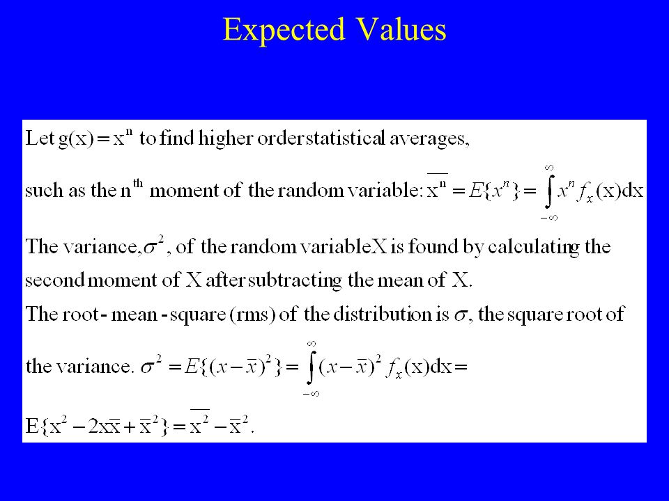
Expected Values

7
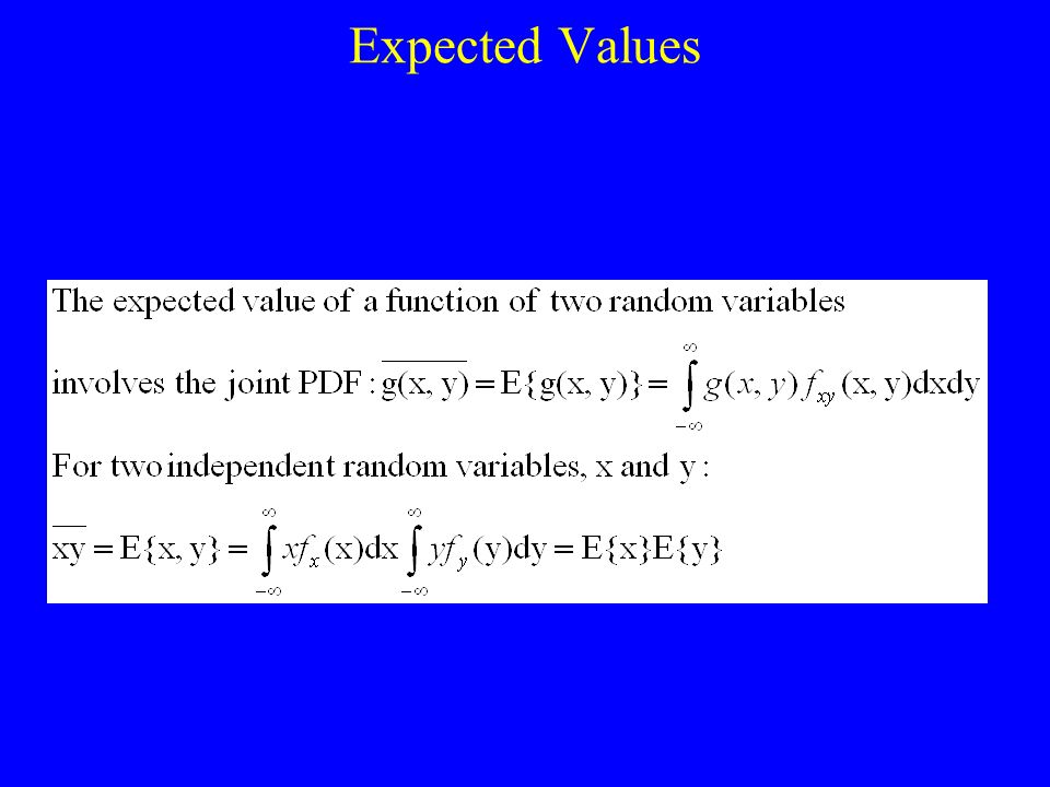
Autocorrelation and Power Spectral Density

9
Noise in Microwave Circuits Result of random motions of charges or charge carriers in devices and materials Thermal noise (most basic type) –thermal vibration of bound charges (also called Johnson or Nyquist noise) Shot noise –random fluctuations of charge carriers Flicker noise –occurs in solid-state components and varies inversely with frequency (1/f -noise)
 –thermal vibration of bound charges (also called Johnson or Nyquist noise) Shot noise –random fluctuations of charge carriers Flicker noise –occurs in solid-state components and varies inversely with frequency (1/f -noise)")
10
Noise in Microwave Circuits Plasma noise –random motion of charges in ionized gas such as a plasma, the ionosphere, or sparking electrical contacts Quantum noise –results from the quantized nature of charge carriers and photons; often insignificant relative to other noise sources

11
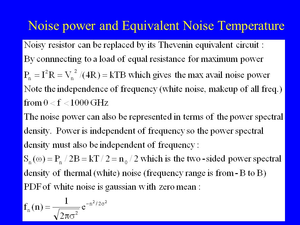
Noise power and Equivalent Noise Temperature

13
Noise in Linear Systems

15
Gaussian white noise through an ideal low-pass filter

16
Gaussian white noise through an ideal integrator

17
Mixing of noise: frequency conversion

19
Basic Threshold Detection

21
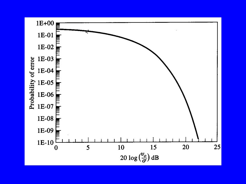
Graphical Representation of Probability of Error for Basic Threshold Detection

23
Noise Temperature and Noise Figure

24
Noise Figure Noisy Rf and microwave components can be characterized by an equivalent noise temperature. An alternative is the noise figure which is the degradation of the signal to noise ratio between the input and the output of the component, or F = (S i /N i )/ (S 0 /N 0 ) 1. The input noise power, N i = k T 0 B; P i = S i + N i ; P 0 = S 0 + N 0 ; S 0 = G S i ; N 0 = kGB(T 0 + T e ) ;
/ (S 0 /N 0 ) 1. The input noise power, N i = k T 0 B; P i = S i + N i ; P 0 = S 0 + N 0 ; S 0 = G S i ; N 0 = kGB(T 0 + T e ) ;.")
25
Noise Figure So F = [(S i / k T 0 B)]/ [(G S i / k G B (T 0 + T e )] =(T 0 + T e )/ T 0 = 1 + T e / T 0 1. Or the temperature of the noisy network T e = (F - 1) T 0. Let N added = noise power added by the network, the output noise power, N 0 = G (N i + N added ) So F = [(S i / N i )]/ [(G S i / G (N i + N added )] = 1 + N added / N i
![Noise Figure So F = [(S i / k T 0 B)]/ [(G S i / k G B (T 0 + T e )] =(T 0 + T e )/ T 0 = 1 + T e / T 0 1.](http://images.slideplayer.com/24/6970430/slides/slide_25.jpg "Or the temperature of the noisy network T e = (F - 1) T 0. Let N added = noise power added by the network, the output noise power, N 0 = G (N i + N added ) So F = [(S i / N i )]/ [(G S i / G (N i + N added )] = 1 + N added / N i.")
26
Noise Figure of a Lossy Line Lossy transmission line (attenuator) held at a physical temperature, T. Power Gain, G 1 If the line input is terminated with a matched load at temperature T, then the output will appear as a resistor of value R and temperature T. Output Noise power is the sum of the input noise power attenuated through the lossy line plus the noise power added by the lossy line itself.

27
Noise Figure of a Lossy Line So the output Noise power, N o = kTB = G(kTB + N added ), where N added is the noise generated by the line. Therefore, N added = {(1/G) - 1 }kTB = (L-1) kTB The equivalent noise temperature T e of the lossy line becomes: T e = N added / KB = (L - 1) T; and the noise figure is F = 1 + T e / T 0 = 1 + (L - 1) T / T 0
 - 1 }kTB = (L-1) kTB The equivalent noise temperature T e of the lossy line becomes: T e = N added / KB = (L - 1) T; and the noise figure is F = 1 + T e / T 0 = 1 + (L - 1) T / T 0.")
28
Noise Figure of Cascaded Components Consider a cascade of two components having power gains G 1 and G 2, noise figures F 1 and F 2 and noise temperatures T 1 and T 2. Find overall noise figure, T and noise temperature T of the cascade as if it were the single component with N i = k T 0 B. Using noise temperatures, the noise power at the output of the first stage is N 1 = G 1 k B T 0 + G 1 k B T e1 ; and the output at the second is N 0 = G 2 N 1 + G 2 k B T e2 = G 1 G 2 k B (T 0 + T e1 + T e2 / G 1 )
.")
29
Noise Figure of Cascaded Components For the equivalent single system: N 0 = G 1 G 2 k B (T 0 + T e ) So the noise of the cascade system is T e = T e1 + T e2 / G 1 Recall F = 1 + T e / T 0 so the cascade system F = 1+ T e1 / T 0 + T e2 / (G 1 T 0 ) = F 1 + ( F 2 - 1) / G 1 ; more generally T e = T e1 + T e2 / G 1 + T e3 / (G 1 G 1 ) F = F 1 + ( F 2 - 1) / G 1 + ( F 3 - 1) / G 1 G 2
 So the noise of the cascade system is T e = T e1 + T e2 / G 1 Recall F = 1 + T e / T 0 so the cascade system F = 1+ T e1 / T 0 + T e2 / (G 1 T 0 ) = F 1 + ( F 2 - 1) / G 1 ; more generally T e = T e1 + T e2 / G 1 + T e3 / (G 1 G 1 ) F = F 1 + ( F 2 - 1) / G 1 + ( F 3 - 1) / G 1 G 2")
33
Noise Figure of a Passive Two-Port Network Impedance mismatches may be defined at each port in terms of the reflection coefficients, as shown in the diagram. Assume the network is at temperature, T and the input noise power is N 1 = k T B is applied to the input of the network. The available output noise at port 2 is N 2 = G 21 k T B + G 21 N added the noise generated internally by the network (referenced at port 1). G 21 is the available gain of the network from port 1 to port 2.
. G 21 is the available gain of the network from port 1 to port 2..")
34
Noise Figure of a Passive Two-Port Network The available gain can be expressed in terms of the S-parameters of the network and the port mismatches as G 21 = power available from network divided by power available from source = { |S 21 | 2 (1- | s | 2 )}/ | 1+S 11 s | 2 (1- | out | 2 ) and the output mismatch is out = S 22 + S 12 S 21 s /(1- S 11 s ) From N 2 =k T B, find N added = (1/G 21 -1)k T B, and the equivalent noise temperature is T e = N added /kB = T(1- G 21 )/ G 21, and F = (1/G 21 -1)T/T 0 Can apply to examples mismatched lossy line and Wilkinson power divider.
}/ | 1+S 11 s | 2 (1- | out | 2 ) and the output mismatch is out = S 22 + S 12 S 21 s /(1- S 11 s ) From N 2 =k T B, find N added = (1/G 21 -1)k T B, and the equivalent noise temperature is T e = N added /kB = T(1- G 21 )/ G 21, and F = (1/G 21 -1)T/T 0 Can apply to examples mismatched lossy line and Wilkinson power divider.")
35
Gain Compression General non-linear network with an input voltage v i and and output voltage v 0 can be expressed in a Taylor series expansion: v 0 = a 0 + a 1 v i + a 2 v i 2 + a 3 v i 3 + … where the Taylor coefficients are given by: a 0 = v 0 (0) (DC output); {rectifier converting ac to dc} a 1 = dv 0 / dv i | v i =0 (linear output) ; {linear attenuator or amplifier} a 2 = d 2 v 0 / dv i 2 | v i =0 (squared output) ; {mixing and other frequency conversion functions}
 (DC output); {rectifier converting ac to dc} a 1 = dv 0 / dv i | v i =0 (linear output) ; {linear attenuator or amplifier} a 2 = d 2 v 0 / dv i 2 | v i =0 (squared output) ; {mixing and other frequency conversion functions}")
36
Gain Compression Let v i = V 0 cos 0 t then evaluate v 0 = a 0 + a 1 v i + a 2 v i 2 + a 3 v i 3 + … v 0 = a 0 + a 1 V 0 cos 0 t + a 2 V 0 2 cos 2 0 t + a 3 V 0 3 cos 3 0 t + … =( a 0 + ½ a 2 V 0 2 ) + (a 1 V 0 + ¾ a 3 V 0 3 ) cos 0 t + ½ a 2 V 0 2 cos 2 0 t + ¼ a 3 V 0 3 cos 3 0 t + … This result leads to the voltage gain of the signal component at frequency 0 G v = v 0 ( 0 ) / v i ( 0 ) = (a 1 V 0 + ¾ a 3 V 0 3 ) / V 0 = a 1 + ¾ a 3 V 0 2 (retaining only terms through the third order)
 + (a 1 V 0 + ¾ a 3 V 0 3 ) cos 0 t + ½ a 2 V 0 2 cos 2 0 t + ¼ a 3 V 0 3 cos 3 0 t + … This result leads to the voltage gain of the signal component at frequency 0 G v = v 0 ( 0 ) / v i ( 0 ) = (a 1 V 0 + ¾ a 3 V 0 3 ) / V 0 = a 1 + ¾ a 3 V 0 2 (retaining only terms through the third order)")
37
Gain Compression G v = v 0 ( 0 ) / v i ( 0 ) = (a 1 V 0 + ¾ a 3 V 0 3 ) / V 0 = a 1 + ¾ a 3 V 0 2 here we see the a 1 term plus a term proportional to the square of the magnitude of the amplitude of the input voltage. The coefficient a 3 is typically negative; so the gain of the amplifier tens to decrease for large values of V 0. This is gain compression or saturation.

38
Intermodulation Distortion For a single input frequency, or tone, 0, the output will consist of harmonics of the input signal of the form, n 0, for n = 0, 1, 2, …. Usually these harmonics are out of the passband of the amplifier, but that is not true when the input consists of two closely spaced frequencies. Let v i = V 0 (cos 1 t + cos 2 t ); where 1 ~ 2. Recall v 0 = a 0 + a 1 v i + a 2 v i 2 + a 3 v i 3 + … ; hence
; where 1 ~ 2. Recall v 0 = a 0 + a 1 v i + a 2 v i 2 + a 3 v i 3 + … ; hence.")
39
Intermodulation Distortion The output spectrum consists of harmonics of the form, m 1 +n 2 with m, n = 0, 1, 2, 3, … These combinations of the two input frequencies are call intermodulation products, with order |m| + |n|. Generally, they are undesirable; however, in cases, for example a mixer, the the sum or difference frequencies form the desired outputs. Note that they are both far from 1 and 2. But the terms 2 1 - 2 and 2 2 - 1 are close to 1 and 2. Which causes third-order intermodulation distortion.

40
Third-Order Intercept Point Plot of first and third-order products of the output versus input power on a log-log plot hence the slopes represent the powers.

41
Dynamic Range

Similar presentations


xy = f(x) Any f(x) can be represented as a Taylor series expansion: a 0 represents a DC offset a 1 represents the linear gain a 2 represents the 2.>")


