Download presentation
Presentation is loading. Please wait.

1
Metrology Roadmap 2000 Update EuropeAlec Reader (Philips) Wilfried Vandervorst (IMEC) Rudolf Laubmeier (Infineon) Rudolf Laubmeier (Infineon) JapanFumio Mizuno (Hitachi) Korea Taiwan Henry Ma (EPISIL) USBob Scace (NIST) Alain Diebold (Int. SEMATECH)
.")
2
AGENDA 1999 ITRS 2000 Review (Why RED?) Requirements Tables for 2000 & 2001
 Requirements Tables for 2000 & 2001")
3
1999 Metrology Roadmap Highlights

4
Why are CD Measurement Requirements RED? There is no universal metrology solution for all CD measurements. –e.g., Scatterometry meets Focus-Exposure precision needs to (70 nm node?) for resist lines but not for contacts (yet). 3D info needed for undercut gate, contact, and other structures. Precision includes tool matching and near + long term measurement variation.
 for resist lines but not for contacts (yet). 3D info needed for undercut gate, contact, and other structures. Precision includes tool matching and near + long term measurement variation..")
5
CD-SEM a Potential Solution for Wafer and Mask / R&D + Production From Sato and Mizuno, EIPBN 2000, Palm Springs, CA Barriers and Solutions 193 & 157 nm Resist Damage » lower dose images Precision Improvements » new nano-tip source Depth of Focus » new SEM concept needed Ultimate Limit of CD-SEM » ~ 5 nm for etched poly Si Gate

6
High Resolution High Depth of FieldLow Beam Energy PICK ANY TWO Many Thanks to David Joy High Voltage ~200 keV is limited to 1 nm resolution for SE imaging

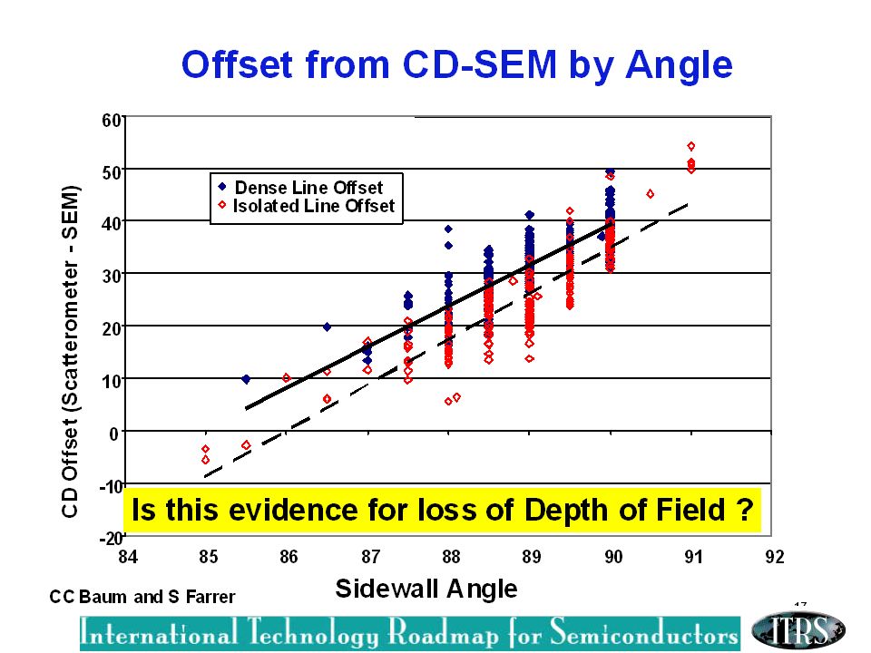
7
Ultimate limit of CD-SEM 20nm TBW = 10 nm CD Gabors limit 5 nm TBW = CD The limit of CD -SEM is based on Secondary Electron resolution is the range of secondary electrons in the material Many Thanks to David Joy

9
60nmnode130 / 90nmnode 40nmnode Schottky Emitter Anode Final Aperature Detector Magnetic Lens Electrostatic Lens Specimen Z U col U E CD-SEM Depth of Field vs Resolution Damage to 193 Resist from e beam & DoF Structure Coherent Electron Beam illumination footprint detector e holography CD Potential Solutions for Mask and Wafer

10
60nmnode130 / 90nmnode 40nmnode Schottky Emitter Anode Final Aperature Detector Magnetic Lens Electrostatic Lens Specimen Z U col U E CD-SEM Depth of Focus vs Resolution Damage to 193 Resist from e beam & DoF Structure Coherent Electron Beam illumination footprint detector e holography Boot Tip Line Scan CD-AFM Tip technology low throughput Tip Technology scatterometry Metal Gates 0th order Incident Laser Beam contacts CD Potential Solutions for Mask and Wafer

11
Materials Characterization Enables Process and Metrology Development Oxynitride and High k Interfaces Dave Muller - Lucent NRA Total N in oxynitride

12
Reason for Red is Precision and Tool Matching IR or UV for In-Line ? Existing in-line metrology 60nmnode 130 / 90nmnode 40nmnode Gate Dielectric Metrology Potential Solutions Enable High k Development with Existing Tool

13
Interconnect Metrology Solutions Barrier/Seed Cu Films 5 Potential Solutions all expected to meet precision requirements some are extendable to patterned wafers Acoustic ISTS Picosecond acoustics X-ray reflectivity X-ray fluorescence Non-contact resistivity

14
Metrology & New Structures Gate Drain Source Vertical Transistor CD is a Film Thickness Courtesy Rafi Kleiman Lucent

15
2000 and 2001 Changes Accelerated Timeline Brings RED closer……….. Developments in some CD measurements push Red out further for some applications?

16
Metrology Challenges by 2000 ITRS Node Timing Brings RED Closer

Similar presentations

 Mauro Vasconi (ST)>")


 Dick Verkleij (Philips) Mauro Vasconi (ST) JapanYuichiro Yamazaki (Toshiba)>")


 Mauro Vasconi (ST) JapanMasahiko Ikeno (Mitsubishi) Toshihiko Osada (Fujitsu) Akira Okamoto.>")


 Ulrich Mantz (Infineon) Vincent Vachellerie (ST) Vincent Vachellerie (ST)JapanKorea Taiwan Henry.>")

 JapanYuichiro Yamazaki (Toshiba) Eiichi Kawamura (Fujitsu Microelectronics) Masahiko Ikeno.>")

