Download presentation
Presentation is loading. Please wait.

1
MOS Transistors The gate material of Metal Oxide Semiconductor Field Effect Transistors was original made of metal hence the name. Present day devices’ gate material is polycrystalline silicon (polysilicon). The transistor (nMOS or pMOS) is a 4-terminal device. n + (nMOS) or p + (pMOS) regions can be considered interchangeable in definining the drain and source terminals.
. The transistor (nMOS or pMOS) is a 4-terminal device. n + (nMOS) or p + (pMOS) regions can be considered interchangeable in definining the drain and source terminals..")
2
Transistor Operation (Simplistic View) The gate is a control input. For the n-type device we have that if the gate voltage is raised it creates an electric field that starts to attract free electrons to the Si-SiO2 interface. Further increase of the gate voltage results in a thin region under the gate being inverted to an n-type semiconductor. This forms a conducting path of electron carriers between source and drain. For digital circuits we simplify the transistor operation such that a voltage value equivalent to the power supply voltage applied to the gate terminal is logic 1 and implies that the switch is ON. This condition allows a logic 1 or logic 0 at the drain to be transferred to the source. A logic 0 applied to the gate of the pMOS implies that the device is ON. The pMOS is OFF otherwise.

3
CMOS Logic Complementary Metal Oxide Semiconductor (CMOS), implies that for every n-type device on a circuit there is a p- type device. Examples are inverters, NAND, AND, NOR, OR etc. An n-input NAND will have n pMOS devices and n nMOS devices. In general CMOS circuits have a pull-up (pMOS) and a pull- down (nMOS) network. An inverter has 4 possible output states namely the crowbarred (X), logic 1, logic 0 and high impedance (Z) How?. Observe that two or more n- type or p-type transistors placed in series constitute an ANDing operation while devices placed in parallel constitute an OR function. This observation allows for the construction of compound gates
 and a pull- down (nMOS) network. An inverter has 4 possible output states namely the crowbarred (X), logic 1, logic 0 and high impedance (Z) How . Observe that two or more n- type or p-type transistors placed in series constitute an ANDing operation while devices placed in parallel constitute an OR function. This observation allows for the construction of compound gates.")
4
Compound Gates Given the function: F = D + A(B + C) We desire to represent this expression using CMOS logic. We apply De Morgan’s theorems to get: F = D(A + BC) The function above represents the pull-up network. The original function un- complemented represents the pull-down network. Key in the synthesis of a complex CMOS gate is to note that the pull-up network is the dual of the pull-down network. Complementary CMOS is naturally inverting and thus implements only functions such as NAND, NOR and XNOR. Noninverting Boolean functions (AND, OR or XOR) cannot represented in CMOS in a single stage. They require an additional inverting stage.
 The function above represents the pull-up network. The original function un- complemented represents the pull-down network. Key in the synthesis of a complex CMOS gate is to note that the pull-up network is the dual of the pull-down network. Complementary CMOS is naturally inverting and thus implements only functions such as NAND, NOR and XNOR. Noninverting Boolean functions (AND, OR or XOR) cannot represented in CMOS in a single stage. They require an additional inverting stage..")
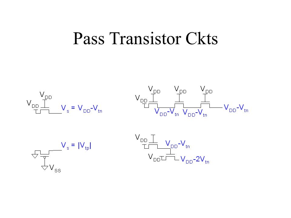
5
Pass Transistors A logic 1 will drive a significant capacitive load in a shorter time if the voltage of the signal is close to the power supply voltage V DD. Similarly a logic 0 will quickly discharge a capacitor if it is as near to 0V as possible. An nMOS device is a near perfect switch for transmitting logic 0 while the pMOS is good for transmitting logic 1. The nMOS degrades a logic 1 as does the pMOS a logic 0. Not such a great idea since we can neither pass good zeros or ones. IN V OUT

6
Pass Transistors Scenario above assumes a grounded source What if source > 0 i.e. both source and drain can attain a value greater than 0? –e.g. pass transistor passing V DD

7
Pass Transistors V g = V DD –If V s > V DD -V t, V gs < V t –Hence transistor would turn itself off nMOS pass transistors pull no higher than V DD -V tn –Called a degraded “1” –Approach degraded value slowly (low I ds ) pMOS pass transistors pull no lower than V tp
 pMOS pass transistors pull no lower than V tp")
8
Pass Transistor Ckts

10
Pass Transistor Logic Sometimes we have a need to pass a signal based on a clock or trigger’s arrival at the gate of a pass transistor. The transistor between the inverters is a pass transistor. It serves to pass D to the input of inverter 2. We can prevent the degradation of D, by using a Complementary Switch (C- Switch). We are now in a position to pass both good 1s and 0s. D CLK D
. We are now in a position to pass both good 1s and 0s. D CLK D.")
11
Multiplexers Complementary switches may be used to select between a number of inputs, thus forming a multiplexer function. Provide the Equation for the 4:1 mux below. For the multiplexer shown we can improve signal integrity by using complementary switches. Memories can also be designed using these switches. A D-Latch would consist of a data input (D), clock input (CLK) and outputs Q and its inverse. A D-Latch is considered level sensitive if the state of the output is dependant on the level of the clock signal. By combining two level sensitive latches with one changing the output state when the clock is at logic 1 while the other changes when the clock is at logic 0, one may construct an edge triggered register. S1S1 S2S2 S1S1 S2S2 V out A B C D
, clock input (CLK) and outputs Q and its inverse. A D-Latch is considered level sensitive if the state of the output is dependant on the level of the clock signal. By combining two level sensitive latches with one changing the output state when the clock is at logic 1 while the other changes when the clock is at logic 0, one may construct an edge triggered register. S1S1 S2S2 S1S1 S2S2 V out A B C D.")
12
Latches and Flip-Flops Refer to text book for the construction of an edge triggered D Register. The figure shows a positive level sensitive latch. The Figure above depicts an edge triggered flip-flop if single phase clocking is used. Two phase clocking alleviates to some degree the set-up and hold time issues. CLK D Q Q D phi 1 Q phi 2 Q

Similar presentations