Download presentation
Presentation is loading. Please wait.

1
Cavity package T.Saeki BCD meeting 20 Dec 2005

2
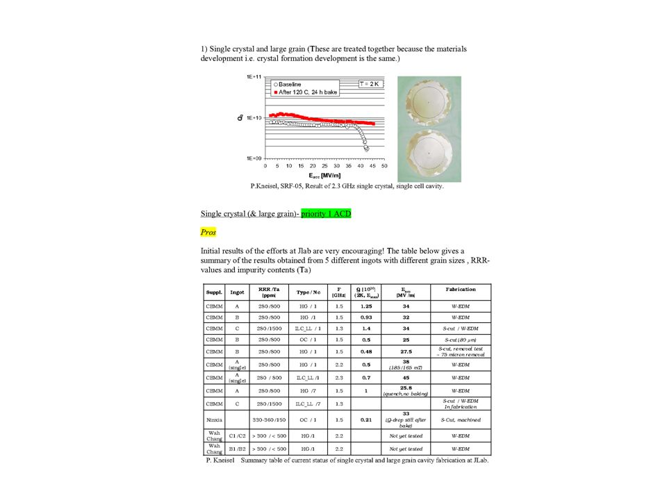
Cavity shape BCD: TESLA shape Pros: small wakefield, HOM thoroughly investigated single-cell: 43 MV/m 9-cell: 40 MV/m (Q=10**10) Cavities and modules have operated in TTF. Cons: high Epk/Eacc ACD1: KEK/DESY low-loss shape Pros: low Hpk/Eacc single-cell: 45-47 MV/m 9-cell: fabricated and tested. Cons: high Epk/Eacc, small aperture ACD2: Cornell Re-entrant shape Pros: low Hpk/Eacc single-cell: 52 MV/m 9-cell: fabrication underway Cons: high Epk/Eacc, HPR problematic

3
Cavity-shape designs with low Bpeak/Eacc made the breakthrough.

5
ACD3: Superstructure pairs of 9-cell cavities. (two pairs of 7-cell cavities studied at DESY) Pros. Cost savings : ½ of input couplers (8000 couplers) Wake-fields are less. Cons. How to process/test a long assembly (BCP, EP, etc…) Cavity shape
 Wake-fields are less. Cons. How to process/test a long assembly (BCP, EP, etc…) Cavity shape.")
6
Cavity material BCD: Nb fine grain sheet Pros: Best known material Cons: Expensive rolling, cleaning and annealing steps. R&D: Impurity of Ta, how many melts, EBM conditions etc. ACD1: Large grain /single crystal (Jlab, DESY, Cornell, FNAL) Pros: Simplification of fabrication and processing => cost savings Potential elimination of EP => Only BCP Cons: Little experience R&D: Acceptable yield strength of material after cut from ingot Cutting techinque: wire EDM is slow ACD2: Nb/Cu clad Pros: Saving Nb material => Cost savings. No EBW at equator, comparable performance to bulk Nb cavity. 3-cell cavity demonstration by DESY. Cons: Contamination risk at welding of endgroup. => Sputterd Nb on Cu with endgroup flanged to cell-structure. Complex cool down (Thermo-current/frozen-in flux)
 Pros: Simplification of fabrication and processing => cost savings Potential elimination of EP => Only BCP Cons: Little experience R&D: Acceptable yield strength of material after cut from ingot Cutting techinque: wire EDM is slow ACD2: Nb/Cu clad Pros: Saving Nb material => Cost savings. No EBW at equator, comparable performance to bulk Nb cavity. 3-cell cavity demonstration by DESY. Cons: Contamination risk at welding of endgroup. => Sputterd Nb on Cu with endgroup flanged to cell-structure. Complex cool down (Thermo-current/frozen-in flux).")
8
Fundamental Material R&D Understanding of underlying physics (purity, grain, surface...) 1) RF critical magnetic Field Ultimate Eacc is limited by Hpk ~ 185 mT. Theory is still under debate. 2) Field emission Eacc > 45 MV/m => Epk > 100 MV/m Control of contamination, clean processing/assemble 3) Defects in material Quench below H(RF) < Hpk. Need scanning method for the defects of <10um. 4) Q-drop (20 – 25 MV/m) Cryo-loss is large. In-stu baking at ~120 deg. C.(>12 hrs) 5) Residual resistance A few n ohms is not on regular basis.
 Field emission Eacc > 45 MV/m => Epk > 100 MV/m Control of contamination, clean processing/assemble 3) Defects in material Quench below H(RF) < Hpk. Need scanning method for the defects of <10um. 4) Q-drop (20 – 25 MV/m) Cryo-loss is large. In-stu baking at ~120 deg. C.(>12 hrs) 5) Residual resistance A few n ohms is not on regular basis..")
9
Cavity Fabrication BCD: Bulk fine-grained Nb sheet, Machining, deep draw forming, Mechanical polishing, pre-cleaning, EBW, inelastic deformation tuning with appropriate intermediate cleaning steps. Options: 1) fine-grain sheet deep drawing + EBW => spinning deep drawing + EBW => hydro-forming endgroup => Nb film on Cu + flanges 2) large/single grain sheet Wire EDM cut of ingot to form sheet 3)Bulk Nb/Cu clad material deep drawing + EBW => hydro-form Nb/Cu clad pipe (9-cell + beam-tubes ???)
 fine-grain sheet deep drawing + EBW => spinning deep drawing + EBW => hydro-forming endgroup => Nb film on Cu + flanges 2) large/single grain sheet Wire EDM cut of ingot to form sheet 3)Bulk Nb/Cu clad material deep drawing + EBW => hydro-form Nb/Cu clad pipe (9-cell + beam-tubes ).")
10
Cavity Fabrication ACD1: Hydro-forming of cell-structure (DESY, KEK) Single-cell cavity: 42 MV/m, Q = 10**10 (KEK & DESY) 3-cell cavity : fabricated. Pros: Saving fabrication cost. Nb material reduction by 75%. Adoidance of machining. Automation. Etc… Cons: Endgroup welding. Contamination of Cu. R&D: Magnetic flux trap by Nb/Cu thrmo-coupling. CARE program in Europe. Bulk Nb seamless 9-cell cavity installation in the cryomodule (2006) ACD2: Spining (INFN) Single-cell cavity: 40 MV/m (INFN) 9-cell cavity: fabricated. Pros: Saving fabrication costs. Cons: Need removal of fissures by substantial grinding. ACD3: Nb films on Cu for endgroups (KEK) Pros: Successful SC flanging => new type of modularity. Inspection, cleaning, assembly separately. Cost savings (Nb and EBW => Cu and brazing) Cons: Complex shape of endgroup => difficult Nb coating. Additional complexity in SC joint.
 ACD2: Spining (INFN) Single-cell cavity: 40 MV/m (INFN) 9-cell cavity: fabricated. Pros: Saving fabrication costs. Cons: Need removal of fissures by substantial grinding. ACD3: Nb films on Cu for endgroups (KEK) Pros: Successful SC flanging => new type of modularity. Inspection, cleaning, assembly separately. Cost savings (Nb and EBW => Cu and brazing) Cons: Complex shape of endgroup => difficult Nb coating. Additional complexity in SC joint..")
11
Cavity preparation BCD: 1)Leak check, mechanical checks, inspection 2)Freq. tuning, field flatness 3)Cleaning 4)Damage layer removal 5)Furnace treatment 6)Final freq. tuning, field flatness 7)Final surface preoparation 8)Final cleaning 9)Bake-out at 120 -130 deg C. 10)Low-power acceptance tests 11)Tank-welding 12)Assembly for high-power operation 13)High-power test
Cleaning 4)Damage layer removal 5)Furnace treatment 6)Final freq. tuning, field flatness 7)Final surface preoparation 8)Final cleaning 9)Bake-out at deg C. 10)Low-power acceptance tests 11)Tank-welding 12)Assembly for high-power operation 13)High-power test.")
12
Cavity preparation ACD1: post-purification at 1400 deg C with Ti. ACD2: Eliminate outside etching ACD3: Hot water rinsing ACD4: Tumbling/barrel polishing to reduce amount of EP necessary (KEK) ACD5: Dry-ice cleaning instead of HPR (DESY) ACD6: Air baking out instead of in-situ vacuum bake at 120 – 130 deg C.
 ACD5: Dry-ice cleaning instead of HPR (DESY) ACD6: Air baking out instead of in-situ vacuum bake at 120 – 130 deg C..")
Similar presentations


, F. Furuta (1), K. Saito (1), M. Ge.>")


 Sokendai, The graduated university for advanced studies. KEK, LL / Ichiro Cavity Group October 21,>")


 STF CM-1 cavities are; MHI-014: 3-rd VT:36MV/m (finished) MHI-015: 3-rd VT: 33.5 -> 18.4MV/m.>")

 in cooperation with Japanese Industries IPAC-2010 Satellite Workshop, Kyoto, May 23, 2010 -A Satellite Workshop at IPAC-2010 - Superconducting.>")

 GDE Mar 3-6, 2008.>")


 ILWS08 in Chicago 17-Nov-08.>")
 Processing of materials SRF materials Workshop Fermilab May 23-24, 2007 Today’s process is long, complex,>")