Download presentation
Presentation is loading. Please wait.

1
Photoluminescence and lasing in a high-quality T-shaped quantum wires M. Yoshita, Y. Hayamizu, Y. Takahashi, H. Itoh, and H. Akiyama Institute for Solid State Physics, Univ. of Tokyo and CREST, JST L. N. Pfeiffer and K. W. West Bell Laboratories, Lucent Technologies NSF-MEXT symposium at Shinagawa, Tokyo (2004.10) 1. Characterization of T-wires, single-T-wire lasers AFM, PL, PLE, PL scan, Lasing 2. Exciton, biexciton, and plasma in quantum wires PL, Absorption/Gain (by Cassidy’s method & Transmission experiment) 3. Exciton Mott transition picture does not seem to work!
 1. Characterization of T-wires, single-T-wire lasers AFM, PL, PLE, PL scan, Lasing 2. Exciton, biexciton, and plasma in quantum wires PL, Absorption/Gain (by Cassidy’s method & Transmission experiment) 3. Exciton Mott transition picture does not seem to work!.")
2
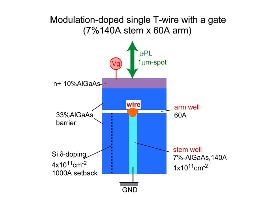
T-shaped Quantum Wire (T-wire)
")
3
Cleaved-edge overgrowth with MBE In situ Cleave (001) MBE Growth (110) MBE Growth [110] [001] GaAs substrate 600 o C490 o C by L. N. Pfeiffer et al., APL 56, 1679 (1990).
![Cleaved-edge overgrowth with MBE In situ Cleave (001) MBE Growth (110) MBE Growth [110] [001] GaAs substrate 600 o C490 o C by L.](http://images.slideplayer.com/23/6876205/slides/slide_3.jpg "N. Pfeiffer et al., APL 56, 1679 (1990)..")
4
490 o C Growth High Quality T-wire Interface control by growth-interruption annealing (by M. Yoshita et al. JJAP 2001) Atomically flat interfaces 600 o C Anneal arm well 6nm stem well 14nm
 Atomically flat interfaces 600 o C Anneal arm well 6nm stem well 14nm.")
5
(Akiyama et al. APL 2003) PL and PLE spectra 1D free exciton small Stokes shift 1D continuum states arm well stem well T-wire
 PL and PLE spectra 1D free exciton small Stokes shift 1D continuum states arm well stem well T-wire.")
6
E-field // to wire _ to wire // to arm well I E-field

7
Cavity length 500 m Probability of Photon Probability of Electron Single quantum wire laser =5x10 -4

8
Scanning micro-PL spectra Continuous PL peak over 20 m PL width < 1.3 meV scan T=5K T-wire stem well

9
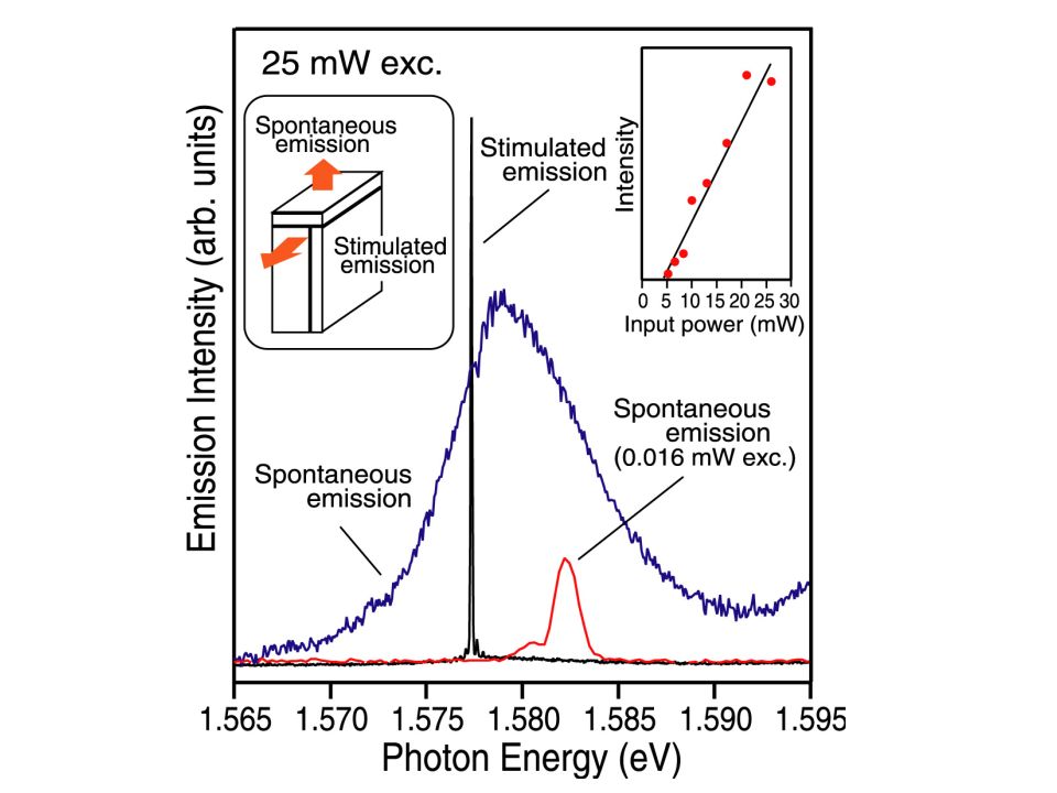
500 m gold-coated cavity Threshold 5mW (Hayamizu et al, APL 2002) Lasing in a single quantum wire
 Lasing in a single quantum wire")
11
Excitation power dependence of PL M. Yoshita, et al.

12
Free Exciton Biexciton+Exciton Electron-hole Plasma Density n 1D = 3.6 x 10 3 cm -1 (r s = 220 a B ) n 1D = 1.2 x 10 5 cm -1 (r s = 6.6 a B ) n 1D = 1.2 x 10 6 cm -1 (r s = 0.65 a B ) n 1D ~ 10 2 cm -1 a B ~13nm E B =2.8meV
 n 1D = 1.2 x 10 5 cm -1 (r s = 6.6 a B ) n 1D = 1.2 x 10 6 cm -1 (r s = 0.65 a B ) n 1D ~ 10 2 cm -1 a B ~13nm E B =2.8meV")
13
Exciton band edge & plasma band edge (T=30K) ▼ plasma band edge (low energy edge of plasma PL) starts at biexciton energy and shows red shift. ▼ exciton band edge, (onset of continuum states) exciton ground and excited states show no shift.
 exciton ground and excited states show no shift..")
14
Excitation Light : cw TiS laser at 1.631eV Waveguide Emission Polarization parallel to Arm well Stripe shape Spectrometer with spectral resolution of 0.15 meV Spontaneous emission Measurement of absorption/gain spectrum Cassidy’s Method 8.3mW

15
Absorption/gain spectrum (High excitation power) Electron-Hole Plasma E FE E BE Gain Absorption Hayamizu et al. unpublished 8.3mW

16
1.Exciton peak and continuum onset decay without shift. 2.Gap between exciton and continuum is gradually filled. 3.Exciton changes to Fermi edge Electron-Hole Plasma Exciton Hayamizu et al. unpublished

17
Transmittance for single Takahashi et al. unpublished Coupling efficiency = 20%

18
Absorption for single Takahashi et al. unpublished

19
Absorption at 300 K Takahashi et al. unpublished

20
Experiment for gain

21
Evolution of continuum Takahashi et al. unpublished

22
Lasing & many-body effects in quantum wires E. Kapon et al. (PRL’89) Lasing in excited-states of V-wires W. Wegscheider et al. Lasing in the ground-state of T-wires, no energy shift, (PRL’93) excitonic lasing R. Ambigapathy et al. PL without BGR, strong excitonic effect in V-wires (PRL’97) L. Sirigu et al. (PRB’00) Lasing due to localized excitons in V-wires J. Rubio et al. (SSC’01) Lasing observed with e–h plasma emission in T-wires A. Crottini et al. (SSC’02) PL from exciton molecules (bi-excitons) in V-wires T. Guillet et al. (PRB’03) PL, Mott transition form excitons to a plasma in V-wires H. Akiyama et al. Lasing due to e–h plasma, no exciton lasing in T-wires (PRB’03) F. Rossi and E. Molinari (PRL’96) F. Tassone, C. Piermarocchi, et al. (PRL’99,SSC’99) S. Das Sarma and D. W. Wang (PRL’00,PRB’01) Theories “1D exciton Mott transition”
 Lasing in excited-states of V-wires W. Wegscheider et al. Lasing in the ground-state of T-wires, no energy shift, (PRL’93) excitonic lasing R. Ambigapathy et al. PL without BGR, strong excitonic effect in V-wires (PRL’97) L. Sirigu et al. (PRB’00) Lasing due to localized excitons in V-wires J. Rubio et al. (SSC’01) Lasing observed with e–h plasma emission in T-wires A. Crottini et al. (SSC’02) PL from exciton molecules (bi-excitons) in V-wires T. Guillet et al. (PRB’03) PL, Mott transition form excitons to a plasma in V-wires H. Akiyama et al. Lasing due to e–h plasma, no exciton lasing in T-wires (PRB’03) F. Rossi and E. Molinari (PRL’96) F. Tassone, C. Piermarocchi, et al. (PRL’99,SSC’99) S. Das Sarma and D. W. Wang (PRL’00,PRB’01) Theories 1D exciton Mott transition .")
23
eg. D. W. Wang and S. Das Sarma, PRB 64, 195313 (2001). ・ reduction of exciton binding energy ・ red shift of the band edge (band-gap renormalization (BGR)) Physics of 1D exciton–plasma crossover Increase of e–h pair density causes the exciton Mott transitionOur results show band edge exciton level no energy shift of the exciton band edge No level-crossing between the band edges and the exciton level Exciton-Mott-transition picture does not work. New picture is needed. plasma low-energy edges appear at the bi-exciton energy positions, and show BGR no connection, but coexistence of two band edges
) Physics of 1D exciton–plasma crossover Increase of e–h pair density causes the exciton Mott transitionOur results show band edge exciton level no energy shift of the exciton band edge No level-crossing between the band edges and the exciton level Exciton-Mott-transition picture does not work. New picture is needed. plasma low-energy edges appear at the bi-exciton energy positions, and show BGR no connection, but coexistence of two band edges.")
24
ここまで。 22 分のトーク。

26
X - Charged Exciton X Exciton Electron plasma and minority hole eh ehe eheeeeeeee

27
E f =6meV E f = 2meV m e =0.067 m 0 m h =0.105 m 0 E b =2meV

29
B. W. Hakki and T. L. Paoli JAP. 46 1299 (1974) : Reflectivity : Absorption coeff. D. T. Cassidy JAP. 56 3096 (1984) Absorption/gain measurement based on Cassidy’s analysis of Fabry-Perot-laser emission below threshold Free Spectral Range
 Absorption/gain measurement based on Cassidy’s analysis of Fabry-Perot-laser emission below threshold Free Spectral Range.")
30
Point Absorption Spectrum by Cassidy method Excitation Light : cw TiS laser at 1.631eV Waveguide Emission Polarization parallel to Arm well Spectrometer with spectral resolution of 0.15 meV Cassidy’s Method Single wire laser, uncoated cavity mirrors

31
Absorption at higher temperatures by Cassidy Hayamizu et al. unpublished

32
The gain peaks appear 2meV below biexciton energy. Gain peaks have symmetric shape and no similarity to 1D Density of States. Gain peaks of 20-wires laser The gain peaks are broadened with slight red shifts.

33
Area intensities of PL peaks Lower energy peak ● vs. exciton peak ○ biex+ex pl+ex pl

34
Wire PL : Peak positions & Width biex+ex pl+ex pl Small peak shift Gradual & symmetric broadening

36
Experiment

37
How to derive

38
Absorption for 20

39
Absorption coefficients

40
(001) and (110) surfaces of GaAs (001) (110) [001] [110] [001]
![(001) and (110) surfaces of GaAs (001) (110) [001] [110] [001]](http://images.slideplayer.com/23/6876205/slides/slide_40.jpg "(001) and (110) surfaces of GaAs (001) (110) [001] [110] [001]")
41
(By Yoshita et al. APL 2002)
")
42
T. Guillet et al. (PRB’03) Mott transition form an exciton gas to a dense plasma in very-high-quality V-wire
 Mott transition form an exciton gas to a dense plasma in very-high-quality V-wire.")
43
eg. D. W. Wang and S. Das Sarma, PRB 64, 195313 (2001). ・ red shift of the band edge (band-gap renormalization (BGR)) ・ reduction of exciton binding energy Physical picture of 1D exciton–plasma transition Increase of e–h pair density causes the exciton Mott transition band edge exciton level
) ・ reduction of exciton binding energy Physical picture of 1D exciton–plasma transition Increase of e–h pair density causes the exciton Mott transition band edge exciton level.")
45
(Zn,Cd ) Se/ZnSe samples Thickness 5 nm Quantum well
 Se/ZnSe samples Thickness 5 nm Quantum well")
46
Conclusions Exciton-Mott-transition picture does not work. New picture is needed. 1.As e-h density is increased, exciton peak and exciton band edge (the onset of continuum states above excitons) decay with NO shift. 2.Exciton band edge does NOT connect to plasma band edge (the low-energy edge of plasma). They even co-exist. Therefore, these edges NEVER cross exciton peak. 3.The exciton-plasma evolution is NOT like an abrupt metal- insulator transition, but a gradual crossover. 4.Lasing is caused by plasma gain, but the gain spectral shape is NOT proportional to 1D density of states, probably due to Coulomb interactions. 5.Exciton gradually changes to Fermi edge in plasma. 6.Biexciton PL gradually changes to plasma PL without shift.
 decay with NO shift. 2.Exciton band edge does NOT connect to plasma band edge (the low-energy edge of plasma). They even co-exist. Therefore, these edges NEVER cross exciton peak. 3.The exciton-plasma evolution is NOT like an abrupt metal- insulator transition, but a gradual crossover. 4.Lasing is caused by plasma gain, but the gain spectral shape is NOT proportional to 1D density of states, probably due to Coulomb interactions. 5.Exciton gradually changes to Fermi edge in plasma. 6.Biexciton PL gradually changes to plasma PL without shift..")
Similar presentations


, S.-K. Lee 1), D. Hongxing 2), Z. Chen 2),>")


 2. Singlet and triplet trion states 3. Modulation doped.>")


 Low dimensional materials: Quantum wells,>")


 0.0 ~ 0.8V wire electron density 0 ~ 4×10 5 cm -1 arm electron density 0 ~ 1.3×10 11.>")

