Download presentation
Presentation is loading. Please wait.

1
ECE 4339 L. Trombetta ECE 4339: Physical Principles of Solid State Devices Len Trombetta Summer 2007 Chapter 9: Optoelectronic Devices

2
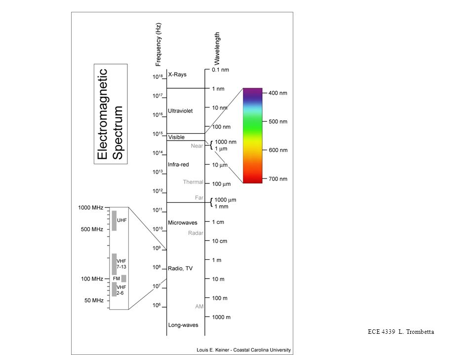
ECE 4339 L. Trombetta

4
Photodiodes Incident light The number of photons decreases exponentially into the material. Also, the absorption rate increases with energy (see Fig. 3.20, next slide) so less light reaches the junction at higher energies.
 so less light reaches the junction at higher energies..")
5
ECE 4339 L. Trombetta

6
The region over which photo-generated electrons and holes are likely to find their way to the depletion region is (L N + W + L P ). Hence where G L is the number of electron/hole pairs created per unit volume per second. The total current is then the sum of I L and whatever current is present with no light (the “dark” current)”: The frequency response of the photodiode is modest: a few 10’s of MHz. If the light intensity is changing faster than that, the photodiode will not respond. This is largely because the diffusion of carriers to the depletion region is slow. Frequency Response
 : The frequency response of the photodiode is modest: a few 10’s of MHz. If the light intensity is changing faster than that, the photodiode will not respond. This is largely because the diffusion of carriers to the depletion region is slow. Frequency Response.")
7
ECE 4339 L. Trombetta The Spectral Response is measured by the current generated as a function of wavelength of incident light. In generating the data, the incident power was the same at all wavelengths, so the number of photons decreases with decreasing wavelength (increasing energy). E EgEg
. E EgEg.")
8
ECE 4339 L. Trombetta Intrinsic region can be “tuned” to the absorption depth of the wavelength of interest. P-I-N Photodiode Response is faster since most electron/hole pairs are generated in the depletion region and do not have to diffuse to it.

9
ECE 4339 L. Trombetta Si Materials issues: some III-V semiconductors have smaller band gaps than Si and can be used at lower wavelengths (for communications applications). But often these need to be deposited on substrates of different materials, so lattice matching becomes an issue. An important materials system is InGaAs – InP.
. But often these need to be deposited on substrates of different materials, so lattice matching becomes an issue. An important materials system is InGaAs – InP..")
10
ECE 4339 L. Trombetta InP is transparent at 1.3 m and 1.55 m, which are important wavelengths for communications applications. In 0.53 Ga 0.47 As is the “active” region. This particular composition is lattice-matched to InP, so defects are minimized. InGaAs – InP p-i-n photodiode

11
ECE 4339 L. Trombetta Fig 6.12 Avalanche Photodiode This diode is operated near avalanche breakdown, so that a small photo-generated current induces avalanche multiplication. This improves the signal/noise ratio.

12
ECE 4339 L. Trombetta Solar Cell For the curve G L = 4G o, the open-circuit voltage and short-circuit current are indicated. The maximum power the cell can deliver is P max = V m I m. I sc V oc max power rectangle ImIm VmVm We define the “fill factor”: Power conversion efficiency:

13
ECE 4339 L. Trombetta Multijunction solar cells use several materials to capture different parts of the solar spectrum.

14
ECE 4339 L. Trombetta http://www.nrel.gov/ncpv/higheff.html Naval Research Labs (NRL) research center: “NREL's record-breaking triple-junction cell uses GaInP (1.8 electron-volt [eV] band gap) to absorb ultraviolet and visible-light wavelengths. The GaAs (1.4-eV band gap) layer absorbs near-infrared light, and the Ge layer absorbs the remaining lower-energy infrared light that still exceeds its 0.7-eV band gap.”
 research center: NREL s record-breaking triple-junction cell uses GaInP (1.8 electron-volt [eV] band gap) to absorb ultraviolet and visible-light wavelengths. The GaAs (1.4-eV band gap) layer absorbs near-infrared light, and the Ge layer absorbs the remaining lower-energy infrared light that still exceeds its 0.7-eV band gap. .")
15
ECE 4339 L. Trombetta

16
LED

17
ECE 4339 L. Trombetta

18
Streetman, “Solid State Electronic Devices”, 4ed., Prentice Hall

Similar presentations


>")


 Low dimensional materials: Quantum wells,>")

