Download presentation
Presentation is loading. Please wait.

1
Cell Architecture

2
Introduction The Cell concept was originally thought up by Sony Computer Entertainment inc. of Japan, for the PlayStation 3 The architecture as it exists today was the work of three companies: Sony, Toshiba and IBM http://www.blachford.info/computer/Cell/Cell0_v2.html http://domino.research.ibm.com/comm/research.nsf/pages/r.arch.innovation.html

3
Why Cell? Sony and Toshiba (being major electronics manufacturers) buy in all manner of different components. One of the reasons for Cell's development is they want to save costs by building their own components. Next generation consumer technologies such as Blu-ray, HDTV, HD Camcorders and of course the PS3 will all require a very high level of computing power and they are going to need the chips to provide it. Cell will be used for all of these and more, IBM will also be using the chips in servers. The partners can also sell the chips to 3rd party manufacturers
 buy in all manner of different components. One of the reasons for Cell s development is they want to save costs by building their own components. Next generation consumer technologies such as Blu-ray, HDTV, HD Camcorders and of course the PS3 will all require a very high level of computing power and they are going to need the chips to provide it. Cell will be used for all of these and more, IBM will also be using the chips in servers. The partners can also sell the chips to 3rd party manufacturers.")
4
What is Cell? Cell is an architecture for high performance distributed computing. It is comprised of hardware and software Cells, software Cells consist of data and programs (known as jobs or apulets), these are sent out to the hardware Cells where they are computed, the results are then returned According to IBM the Cell performs 10x faster than existing CPUs on many applications.
, these are sent out to the hardware Cells where they are computed, the results are then returned According to IBM the Cell performs 10x faster than existing CPUs on many applications..")
5
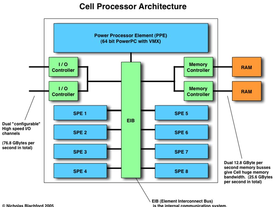
Specifications A hardware Cell is made up of: 1 Power Processor Element (PPE). 8 Synergistic Processor Elements (SPEs). Element Interconnect Bus (EIB). Direct Memory Access Controller (DMAC). 2 Rambus XDR memory controllers. Rambus FlexIO (Input / Output) interface.
. Element Interconnect Bus (EIB). Direct Memory Access Controller (DMAC). 2 Rambus XDR memory controllers. Rambus FlexIO (Input / Output) interface..")
7
Power Processor Element (PPE) The PPE is a conventional microprocessor core which sets up tasks for the SPEs to do. In a Cell based system the PPE will run the operating system and most of the applications but compute intensive parts of the OS and applications will be offloaded to the SPEs. The PPE is a 64 bit, "Power Architecture" processor with 512K cache. While the PPE uses the PowerPC instruction set, it is not based on an existing design on the market today. That is to say, it is NOT based on the existing 970 / G5 or POWER processors. It is a completely different architecture so clock speed comparisons are completely meaningless.

8
Power Processor Element (PPE) The PPE is a dual issue, dual threaded, in-order processor. Unlike many modern processors the hardware architecture is an “old style” RISC design, i.e. the PPE has a relatively simple architecture. Most modern microprocessors devote a large amount of silicon to executing as many instructions as possible at once by executing them "out-of-order" (OOO). This type of design is widely used but it requiring hefty amounts of additional circuitry and consumes large amounts of power. With the PPE, IBM have not done this and have instead gone with a much simpler design which uses considerably less power than other PowerPC devices - even at higher clock rates.
. This type of design is widely used but it requiring hefty amounts of additional circuitry and consumes large amounts of power. With the PPE, IBM have not done this and have instead gone with a much simpler design which uses considerably less power than other PowerPC devices - even at higher clock rates..")
9
Power Processor Element (PPE) This design will however have the downside of potentially having rather erratic performance on branch laden applications. Such a simple CPU needs the compiler to do a lot of the scheduling work that hardware usually does so a good compiler will be essential. The Cell's high bandwidth memory and I/O subsystems and the PPE's high clock speed and dual threading capability may well make up for these potential performance deficiencies.

10
Synergistic Processor Elements (SPEs) An SPE is a self contained vector processor which acts as an independent processor. They each contain 128 x 128 bit registers, there are also 4 (single precision) floating point units capable of 32 GigaFLOPS* and 4 Integer units capable of 32 GOPS (Billions of integer Operations per Second) at 4GHz. The SPEs also include a small 256 Kilobyte local store instead of a cache. According to IBM a single SPE (which is just 15 square millimetres and consumes less than 5 Watts at 4GHz) can perform as well as a top end (single core) desktop CPU given the right task.
 floating point units capable of 32 GigaFLOPS* and 4 Integer units capable of 32 GOPS (Billions of integer Operations per Second) at 4GHz. The SPEs also include a small 256 Kilobyte local store instead of a cache. According to IBM a single SPE (which is just 15 square millimetres and consumes less than 5 Watts at 4GHz) can perform as well as a top end (single core) desktop CPU given the right task..")
11
SPE Local Stores Like the PPE, the SPEs are in-order processors and have no Out-Of-Order capabilities. This means that as with the PPE the compiler is very important. The SPEs do however have 128 registers and this gives plenty of room for the compiler to unroll loops and use other techniques which largely negate the need for OOO hardware. One way in which SPEs operate differently from conventional CPUs is that they lack a cache and instead use a “Local Store”. This potentially makes them (slightly) harder to program but they have been designed this way to reduce hardware complexity and increase performance.
 harder to program but they have been designed this way to reduce hardware complexity and increase performance..")
12
Conventional Cache (~recap) Conventional CPUs perform all their operations in registers which are directly read from or written to main memory. Caches (fast on chip memory) are used to hide the effects of going to or from main memory If data being worked on is not present in the cache, the CPU stalls and has to wait for this data to be fetched.
 are used to hide the effects of going to or from main memory If data being worked on is not present in the cache, the CPU stalls and has to wait for this data to be fetched..")
13
Dual Core Cache Dual-core CPUs will become common soon and desktop versions have a cache per core. If either of the cores or other system components try to access the same memory address, the data in the cache may become out of date and thus needs updated (made coherent). Supporting this requires logic and takes time and in doing so this limits the speed that a conventional system can access memory and cache. The more processors there are in a system the more complex this problem becomes. Cache design in conventional CPUs speeds up memory access but compromises are required to make it work.
. Supporting this requires logic and takes time and in doing so this limits the speed that a conventional system can access memory and cache. The more processors there are in a system the more complex this problem becomes. Cache design in conventional CPUs speeds up memory access but compromises are required to make it work..")
14
SPE Local Stores To solve the complexity associated with cache design and to increase performance the Cell designers took the radical approach of not including any. Instead they used a series of 256 Kbyte “local stores”, there are 8 of these, 1 per SPE. Local stores are like cache in that they are an on-chip memory but the way they are constructed and act is completely different. The SPEs operate on registers which are read from or written to the local stores. The local stores can access main memory in blocks of 1Kb minimum (16Kb maximum) but the SPEs cannot act directly on main memory (they can only move data to or from the local stores). Caches can deliver similar or even faster data rates but only in very short bursts (a couple of hundred cycles at best), the local stores can each deliver data at this rate continually for over ten thousand cycles without going to RAM.
 but the SPEs cannot act directly on main memory (they can only move data to or from the local stores). Caches can deliver similar or even faster data rates but only in very short bursts (a couple of hundred cycles at best), the local stores can each deliver data at this rate continually for over ten thousand cycles without going to RAM..")
15
SPE Local Stores One potential problem is that of “contention”. Data needs to be written to and from memory while data is also being transferred to or from the SPE’s registers and this leads to contention where both systems will fight over access slowing each other down. To get around this the external data transfers access the local memory 1024 bits at a time, in one cycle (equivalent to a transfer rate of 0.5 Terabytes per second!). This is just moving data to and from buffers but moving so much in one go means that contention is kept to a minimum.
. This is just moving data to and from buffers but moving so much in one go means that contention is kept to a minimum..")
16
Cell Characteristics A big difference in Cells from normal CPUs is the ability of the SPEs in a Cell to be chained together to act as a stream processor [Stream]. A stream processor takes data and processes it in a series of steps.
![Cell Characteristics A big difference in Cells from normal CPUs is the ability of the SPEs in a Cell to be chained together to act as a stream processor [Stream].](http://images.slideplayer.com/22/6499483/slides/slide_16.jpg "A stream processor takes data and processes it in a series of steps..")
17
Cell Architecture

18
Element Interconnect Bus (EIB) The EIB consists of 4 x 16 byte rings which run at half the CPU clock speed and can allow up to 3 simultaneous transfers. The theoretical peak of the EIB is 96 bytes per cycle (384 Gigabytes per second) however, according to IBM only about two thirds of this is likely to be achieved in practice.
 however, according to IBM only about two thirds of this is likely to be achieved in practice..")
19
Memory and I/O The Cell will use high speed XDR RAM for memory. A Cell has a memory bandwidth of 25.6 Gigabytes per second which is considerably higher than any PC but necessary as the SPEs will eat as much memory bandwidth as they can get. The Cells run its memory interface at 3.2 Gigabits per second per pin though memory in production now is already capable of higher speeds than this. XDR is designed to scale to 6.4 Gigabits per second so memory bandwidth has the potential to double.

Similar presentations


 CS 147 Li-Chuan Fang.>")


