Download presentation
Presentation is loading. Please wait.

1
Lecture 10: Memory Hierarchy Design Kai Bu kaibu@zju.edu.cn http://list.zju.edu.cn/kaibu/comparch

2
Assignment 3 due May 13

3
Chapter 2 Appendix B

4
Memory Hierarchy

5
Virtual Memory Larger memory for more processes

6
Cache Performance Average Memory Access Time = Hit Time + Miss Rate x Miss Penalty

7
Six Basic Cache Optimizations 1. larger block size reduce miss rate; --- spatial locality; reduce static power; --- lower tag #; increase miss penalty, capacity/conflict misses; 2. bigger caches reduce miss rate; --- capacity misses increase hit time; increase cost and (static & dynamic) power; 3. higher associativity reduce miss rate; --- conflict misses; increase hit time; increase power;
 power; 3. higher associativity reduce miss rate; --- conflict misses; increase hit time; increase power;.")
8
Six Basic Cache Optimizations 4. multilevel caches reduce miss penalty; reduce power; average memory access time = Hit time L1 + Miss rate L1 x (Hit time L2 + Miss rate L2 x Miss penalty L2 ) 5. giving priority to read misses over writes reduce miss penalty; introduce write buffer;
 5. giving priority to read misses over writes reduce miss penalty; introduce write buffer;.")
9
Six Basic Cache Optimizations 6. avoiding address translation during indexing of the cache reduce hit time; use page offset to index cache; virtually indexed, physically tagged;

10
Outline Ten Advanced Cache Optimizations Memory Technology and Optimizations Virtual Memory and Virtual Machines ARM Cortex-A8 & Intel Core i7

11
Outline Ten Advanced Cache Optimizations Memory Technology and Optimizations Virtual Memory and Virtual Machines ARM Cortex-A8 & Intel Core i7

12
Ten Advanced Cache Opts Goal: average memory access time Metrics to reduce/optimize hit time miss rate miss penalty cache bandwidth power consumption

13
Ten Advanced Cache Opts Reduce hit time small and simple first-level caches; way prediction; decrease power; Reduce cache bandwidth pipelined/multibanked/nonblocking cache; Reduce miss penalty critical word first; merging write buffers; Reduce miss rate compiler optimizations; decrease power; Reduce miss penalty or miss rate via parallelism hardware/compiler prefetching; increase power;

14
Opt #1: Small and Simple First-Level Caches Reduce hit time and power

15
Opt #1: Small and Simple First-Level Caches Reduce hit time and power

16
Opt #1: Small and Simple First-Level Caches Example a 32 KB cache; two-way set associative: 0.038 miss rate; four-way set associative: 0.037 miss rate; four-way cache access time is 1.4 times two-way cache access time; miss penalty to L2 is 15 times the access time for the faster L1 cache (i.e., two-way) assume always L2 hit; Q: which has faster memory access time?
 assume always L2 hit; Q: which has faster memory access time")
17
Opt #1: Small and Simple First-Level Caches Answer Average memory access time 2-way =Hit time + Miss rate x Miss penalty =1 + 0.038 x 15 =1.38 Average memory access time 4-way =1.4 + 0.037 x (15/1.4) =1.77
 =1.77")
18
Opt #2: Way Prediction Reduce conflict misses and hit time Way prediction block predictor bits are added to each block to predict the way/block within the set of the next cache access the multiplexor is set early to select the desired block; only a single tag comparison is performed in parallel with cache reading; a miss results in checking the other blocks for matches in the next clock cycle;

19
Opt #3: Pipelined Cache Access Increase cache bandwidth Higher latency Greater penalty on mispredicted branches and more clock cycles between issues the load and using the data

20
Opt #4: Nonblocking Caches Increase cache bandwidth Nonblocking/lockup-free cache allows data cache to continue to supply cache hits during a miss;

21
Opt #5: Multibanked Caches Increase cache bandwidth Divide cache into independent banks that support simultaneous accesses Sequential interleaving spread the addresses of blocks sequentially across the banks

22
Opt #6: Critical Word First & Early Restart Reduce miss penalty Motivation: the processor normally needs just one word of the block at a time Critical word first request the missed word first from the memory and send it to the processor as soon as it arrives; Early restart fetch the words in normal order, as soon as the requested word arrives send it to the processor;

23
Opt #7: Merging Write Buffer Reduce miss penalty Write merging merges four entries into a single buffer entry

24
Opt #8: Compiler Optimizations Reduce miss rates, w/o hw changes Tech 1: Loop interchange exchange the nesting of the loops to make the code access the data in the order in which they are stored

25
Opt #8: Compiler Optimizations Reduce miss rates, w/o hw changes Tech 2: Blocking x = y*z; both row&column accesses before

26
Opt #8: Compiler Optimizations Reduce miss rates, w/o hw changes Tech 2: Blocking x = y*z; both row&column accesses after; maximize accesses loaded data before they are replaced

27
Opt #9: Hardware Prefetching Reduce miss penalty/rate Prefetch items before the processor requests them, into the cache or external buffer Instruction prefetch fetch two blocks on a miss: requested one into cache + next consecutive one into instruction stream buffer Similar Data prefetch approaches

28
Opt #9: Hardware Prefetching

29
Opt #10: Compiler Prefetching Reduce miss penalty/rate Compiler to insert prefetch instructions to request data before the processor needs it Register prefetch load the value into a register Cache prefetch load data into the cache

30
Opt #10: Compiler Prefetching Example: 251 misses 16-byte blocks; 8-byte elements for a and b; write-back strategy; a[0][0] miss, copy both a[0][0],a[0][1] as one block contains 16/8 = 2; so for a: 3 x (100/2) = 150 misses b[0][0] – b[100][0]: 101 misses
![Opt #10: Compiler Prefetching Example: 251 misses 16-byte blocks; 8-byte elements for a and b; write-back strategy; a[0][0] miss, copy both a[0][0],a[0][1] as one block contains 16/8 = 2; so for a: 3 x (100/2) = 150 misses b[0][0] – b[100][0]: 101 misses](http://images.slideplayer.com/18/6080412/slides/slide_30.jpg "Opt #10: Compiler Prefetching Example: 251 misses 16-byte blocks; 8-byte elements for a and b; write-back strategy; a[0][0] miss, copy both a[0][0],a[0][1] as one block contains 16/8 = 2; so for a: 3 x (100/2) = 150 misses b[0][0] – b[100][0]: 101 misses")
31
Example: 19 misses Opt #10: Compiler Prefetching 7 misses: b[0][0] – b[6][0] 4 misses: 1/2 of a[0][0] – a[0][6] 4 misses: a[1][0] – b[1][6] 4 misses: a[2][0] – b[2][6]
![Example: 19 misses Opt #10: Compiler Prefetching 7 misses: b[0][0] – b[6][0] 4 misses: 1/2 of a[0][0] – a[0][6] 4 misses: a[1][0] – b[1][6] 4 misses: a[2][0] – b[2][6]](http://images.slideplayer.com/18/6080412/slides/slide_31.jpg "Example: 19 misses Opt #10: Compiler Prefetching 7 misses: b[0][0] – b[6][0] 4 misses: 1/2 of a[0][0] – a[0][6] 4 misses: a[1][0] – b[1][6] 4 misses: a[2][0] – b[2][6]")
32
Outline Ten Advanced Cache Optimizations Memory Technology and Optimizations Virtual Memory and Virtual Machines ARM Cortex-A8 & Intel Core i7

33
Main Memory Main memory: I/O interface between caches and servers Dst of input & src of output Control Datapath Secondary Storage (Disk) Processor Registers Main Memory (DRAM) Second Level Cache (SRAM) On-Chip Cache Fastest Slowest Smallest Biggest Highest Lowest Speed: Size: Cost: Compiler Hardware Operating System
 Processor Registers Main Memory (DRAM) Second Level Cache (SRAM) On-Chip Cache Fastest Slowest Smallest Biggest Highest Lowest Speed: Size: Cost: Compiler Hardware Operating System")
34
Main Memory Performance measures Latency important for caches; harder to reduce; Bandwidth important for multiprocessors, I/O, and caches with large block sizes; easier to improve with new organizations;

35
Main Memory Performance measures Latency access time: the time between when a read is requested and when the desired word arrives; cycle time: the minimum time between unrelated requests to memory; or the minimum time between the start of on access and the start of the next access;

36
Main Memory SRAM for cache DRAM for main memory

37
SRAM Static Random Access Memory Six transistors per bit to prevent the information from being disturbed when read Don’t need to refresh, so access time is very close to cycle time

38
DRAM Dynamic Random Access Memory Single transistor per bit Reading destroys the information Refresh periodically cycle time > access time

39
DRAM Dynamic Random Access Memory Single transistor per bit Reading destroys the information Refresh periodically cycle time > access time DRAMs are commonly sold on small boards called DIMM (dual inline memory modules), typically containing 4 ~ 16 DRAMs
, typically containing 4 ~ 16 DRAMs")
40
DRAM Organization RAS: row access strobe CAS: column access strobe

41
DRAM Organization

42
DRAM Improvement Timing signals allow repeated accesses to the row buffer w/o another row access time; Leverage spatial locality each array will buffer 1024 to 4096 bits for each access;

43
DRAM Improvement Clock signal added to the DRAM interface, so that repeated transfers will not involve overhead to synchronize with memory controller; SDRAM: synchronous DRAM

44
DRAM Improvement Wider DRAM to overcome the problem of getting a wide stream of bits from memory without having to make the memory system too large as memory system density increased; widening the cache and memory widens memory bandwidth; e.g., 4-bit transfer mode up to 16-bit buses

45
DRAM Improvement DDR: double data rate to increase bandwidth, transfer data on both the rising edge and falling edge of the DRAM clock signal, thereby doubling the peak data rate;

46
DRAM Improvement Multiple Banks break a single SDRAM into 2 to 8 blocks; they can operate independently; Provide some of the advantages of interleaving Help with power management

47
DRAM Improvement Reducing power consumption in SDRAMs dynamic power: used in a read or write static/standby power Depend on the operating voltage Power down mode: entered by telling the DRAM to ignore the clock disables the SDRAM except for internal automatic refresh;

48
Flash Memory A type of EEPROM (electronically erasable programmable read-only memory) Read-only but can be erased Hold contents w/o any power
 Read-only but can be erased Hold contents w/o any power")
49
Flash Memory Differences from DRAM Must be erased (in blocks) before it is overwritten Static and less power consumption Has a limited number of write cycles for any block Cheaper than SDRAM but more expensive than disk Slower than SDRAM but faster than disk
 before it is overwritten Static and less power consumption Has a limited number of write cycles for any block Cheaper than SDRAM but more expensive than disk Slower than SDRAM but faster than disk")
50
Memory Dependability Soft errors changes to a cell’s contents, not a change in the circuitry Hard errors permanent changes in the operation of one of more memory cells

51
Memory Dependability Error detection and fix Parity only only one bit of overhead to detect a single error in a sequence of bits; e.g., one parity bit per 8 data bits ECC only detect two errors and correct a single error with 8-bit overhead per 64 data bits Chipkill handle multiple errors and complete failure of a single memory chip

52
Memory Dependability Rates of unrecoverable errors in 3 yrs Parity only about 90,000, or one unrecoverable (undetected) failure every 17 mins ECC only about 3,500 or about one undetected or unrecoverable failure every 7.5 hrs Chipkill 6, or about one undetected or unrecoverable failure every 2 months
 failure every 17 mins ECC only about 3,500 or about one undetected or unrecoverable failure every 7.5 hrs Chipkill 6, or about one undetected or unrecoverable failure every 2 months")
53
Outline Ten Advanced Cache Optimizations Memory Technology and Optimizations Virtual Memory and Virtual Machines ARM Cortex-A8 & Intel Core i7

54
VMM: Virtual Machine Monitor three essential characteristics: 1. VMM provides an environment for programs which is essentially identical with the original machine; 2. programs run in this environment show at worst only minor decreases in speed; 3. VMM is in complete control of system resources; Mainly for security and privacy sharing and protection among multiple processes

55
Virtual Memory The architecture must limit what a process can access when running a user process yet allow an OS process to access more Four tasks for the architecture

56
Virtual Memory 1. The architecture provides at least two modes, indicating whether the running process is a user process or an OS process (kernel/supervisor process) 2. The architecture provides a portion of the processor state that a user process can use but not write 3. The architecture provides mechanisms whereby the processor can go from user mode to supervisor mode (system call) and vice versa 4. The architecture provides mechanisms to limit memory accesses to protect the memory state of a process w/o having to swap the process to disk on a context switch
 2. The architecture provides a portion of the processor state that a user process can use but not write 3. The architecture provides mechanisms whereby the processor can go from user mode to supervisor mode (system call) and vice versa 4. The architecture provides mechanisms to limit memory accesses to protect the memory state of a process w/o having to swap the process to disk on a context switch.")
57
Virtual Machines Virtual Machine a protection mode with a much smaller code base than the full OS VMM: virtual machine monitor hypervisor software that supports VMs Host underlying hardware platform

58
Virtual Machines Requirements 1. Guest software should behave on a VM exactly as if it were running on the native hardware 2. Guest software should not be able to change allocation of real system resources directly

59
Outline Ten Advanced Cache Optimizations Memory Technology and Optimizations Virtual Memory and Virtual Machines ARM Cortex-A8 & Intel Core i7

60
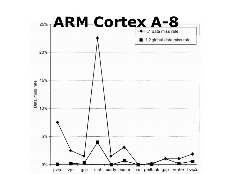
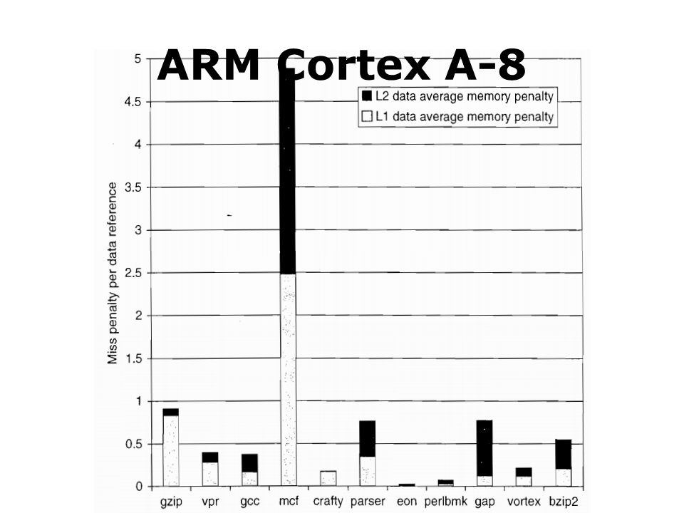
ARM Cortex A-8

63
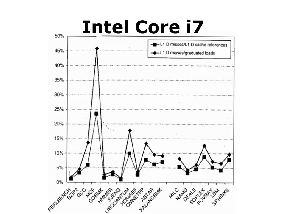
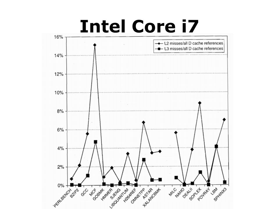
Intel Core i7

66
?

Similar presentations


 Multilevel Caches: A second level cache (L2) is added between the original Level-1 cache and main memory.>")


>")


>")
>")


 DRAM: –value is stored as a charge.>")


