Download presentation
Presentation is loading. Please wait.

1
SEMICONDUCTOR DEVICE FABRICATION AN OVERVIEW Presented to EE 2212 Text Section 2.11 Supplement 24 September 2014

2
OUTLINE èDimensions and Units èWhat is a Monolithic (“Single Stone”) Integrated Circuit (IC)? èFabrication and Integrated Circuit Overview èHistorical Perspectives èPhotolithography èBasic process sequence èPackaging èBasic Processing Steps Summary èOther Devices and Technologies

3
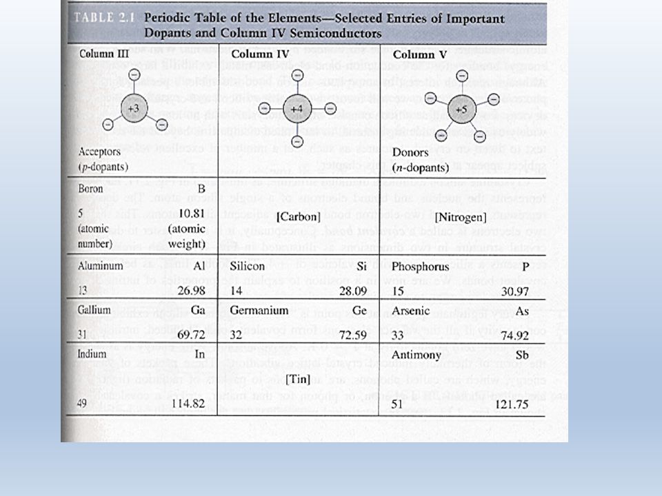
DIMENSIONS AND UNITS 1 micrometer (1 m) = 10 -6 m = 10 -4 cm è1 Å = 10 -10 m = 10 -8 cm (Å =Angstrom) 10,000 Å = 1 m = 1000 nm è1 nanometer (1 nm) = 10 -9 m = 10 Å Wavelength of visible light 0.4 m(violet) to 0.7 m(red) {400 nm to 700 nm, 4,000 Å to 7,000 Å } 1 mil = 0.001 inch = 25.4 m èSheet of notebook paper about 4 mils 1 human hair = 75 m to 100 m = 75,000-100,000 nm èAtomic spacing in a crystal ~ 3 to 5 Å Fingernail growth rate about 1-3 m/hour ( Not personally verified ) èAggressive production minimum feature sizes, tens of nm, 20 nm used in the iPhone 6 A8 microprocessor.
 = m = cm è1 Å = m = cm (Å =Angstrom) 10,000 Å = 1 m = 1000 nm è1 nanometer (1 nm) = m = 10 Å Wavelength of visible light 0.4 m(violet) to 0.7 m(red) {400 nm to 700 nm, 4,000 Å to 7,000 Å } 1 mil = inch = 25.4 m èSheet of notebook paper about 4 mils 1 human hair = 75 m to 100 m = 75, ,000 nm èAtomic spacing in a crystal ~ 3 to 5 Å Fingernail growth rate about 1-3 m/hour ( Not personally verified ) èAggressive production minimum feature sizes, tens of nm, 20 nm used in the iPhone 6 A8 microprocessor.")
4
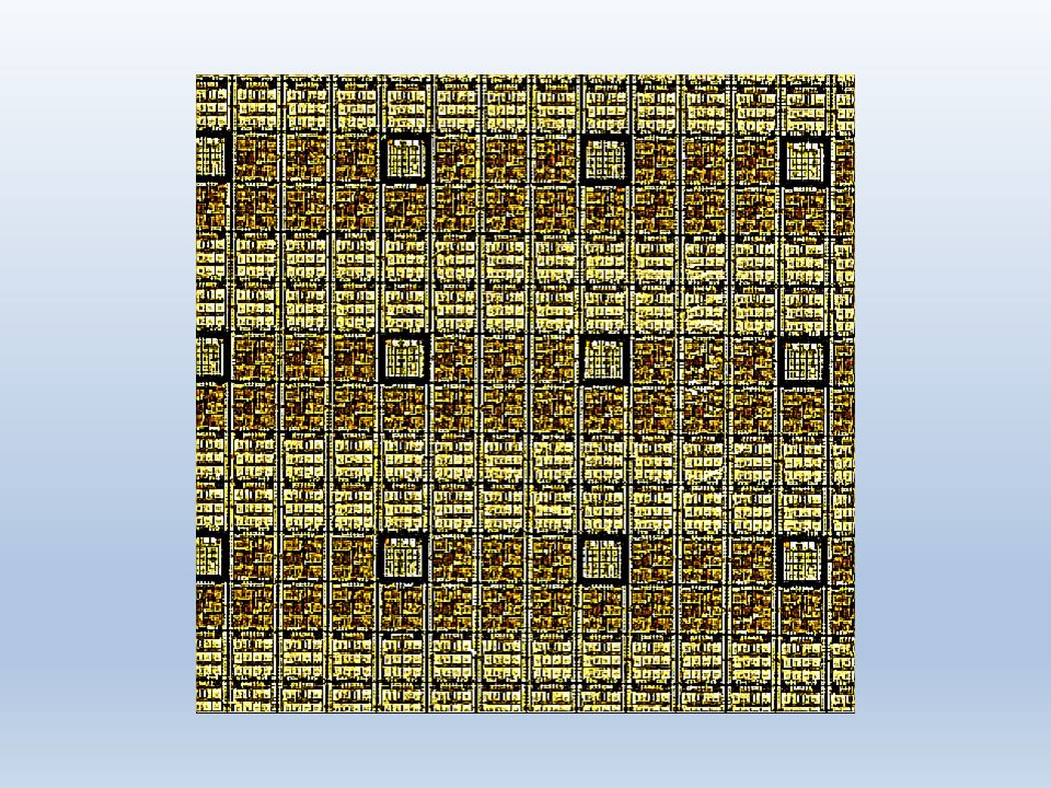
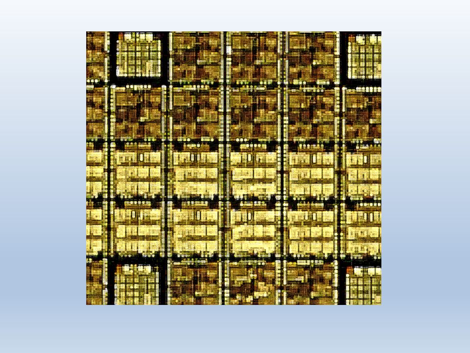
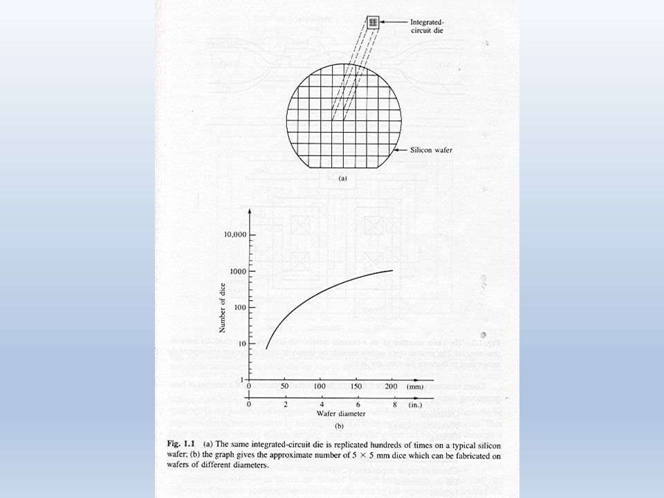
4 IC Fabrication Overview Procedure of Silicon Wafer Production Raw material ― Polysilicon nuggets purified from sand Crystal pulling Si crystal ingot Slicing into Si wafers using a diamond saw Final wafer product after polishing, cleaning and inspection A silicon wafer fabricated with microelectronic circuits Up to you. Keep in touch.

9
Stanley G. Burns UMD-ECE

13
<$50 128 GB 20 nm

19
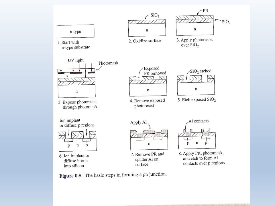
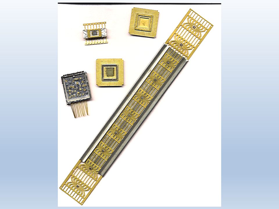
BASIC PROCESSING STEPS Design Then Repeated Application Of: Oxidation and/or Nitridation Photolithography Wet Etching (Chemical) Dry Etching (Plasma) Ion Implantation and/or Diffusion Evaporation Sputtering Plasma Assisted Deposition Epitaxy Many Processing Steps are at temperatures to 1200°C
 Dry Etching (Plasma) Ion Implantation and/or Diffusion Evaporation Sputtering Plasma Assisted Deposition Epitaxy Many Processing Steps are at temperatures to 1200°C")
21
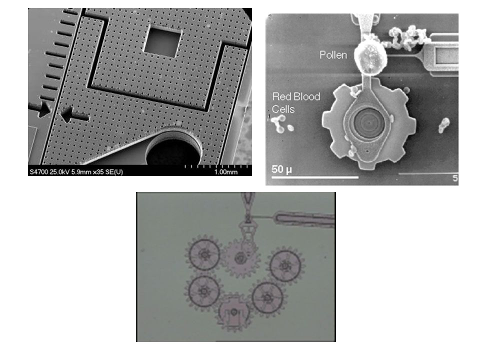
OTHER DEVICES AND TECHNOLOGIES Thin-Film Transistors (TFT) Displays-Liquid Crystal Displays (LCD), Plasma, LED Backlit, etc. Photonic-Light Emitting Diodes (LED), Organic Light Emitting Diodes (OLED), LASERS, Optical Chips, etc.) Photovoltaics-Conventional Crystalline and Flexible Thin-Film Devices and Systems on Flexible Substrates Micro-Electro-Mechanical Systems (MEMS) integration of mechanical elements, sensors, actuators, and electronics on a common silicon substrate through microfabrication technology. Electronics are fabricated using integrated circuit (IC) process sequences (e.g., CMOS, Bipolar, or BICMOS processes) Micromechanical components are fabricated using compatible "micromachining" processes that selectively etch away parts of the silicon wafer or add new structural layers to form the mechanical and electromechanical devices.
, Organic Light Emitting Diodes (OLED), LASERS, Optical Chips, etc.) Photovoltaics-Conventional Crystalline and Flexible Thin-Film Devices and Systems on Flexible Substrates Micro-Electro-Mechanical Systems (MEMS) integration of mechanical elements, sensors, actuators, and electronics on a common silicon substrate through microfabrication technology. Electronics are fabricated using integrated circuit (IC) process sequences (e.g., CMOS, Bipolar, or BICMOS processes) Micromechanical components are fabricated using compatible micromachining processes that selectively etch away parts of the silicon wafer or add new structural layers to form the mechanical and electromechanical devices..")
22
OTHER DEVICES AND TECHNOLOGIES èThin-Film Transistors (TFT) for displays and cameras èDisplays-Liquid Crystal Displays (LCD), Plasma, LED Backlit, etc. Television, computer, and smart phone screens èPhotonic-Light Emitting Diodes (LED), Organic Light Emitting Diodes (OLED), LASERS, Optical Chips, etc.), Lighting èPhotovoltaics-Conventional Crystalline and Flexible Thin-Film èDevices and Systems on Flexible Substrates. Next generation of smart phones èMicro-Electro-Mechanical Systems (MEMS) integration of mechanical elements, sensors, actuators, and electronics on a common silicon substrate through microfabrication technology. Automotive, medical, personal electronics
, Organic Light Emitting Diodes (OLED), LASERS, Optical Chips, etc.), Lighting èPhotovoltaics-Conventional Crystalline and Flexible Thin-Film èDevices and Systems on Flexible Substrates. Next generation of smart phones èMicro-Electro-Mechanical Systems (MEMS) integration of mechanical elements, sensors, actuators, and electronics on a common silicon substrate through microfabrication technology. Automotive, medical, personal electronics.")
Similar presentations
>")


 Electrodes (ode)>")
>")


) 2. Polycrystalline ― with.>")
)>")

