Download presentation
Presentation is loading. Please wait.

1
Voltage or Current References Requirements of a Reference Circuit: Should be independent of power supply Should be independent of temperature Should be independent of processing variations Should be independent of noise

2
Voltage or Current References Requirements of a Reference Circuit: Should be independent of power supply Should be independent of temperature Should be independent of processing variations Should be independent of noise S = ( V ref / V ref ) / ( V dd / V dd ) V dd V ref Sensitivity:
 / ( V dd / V dd ) V dd V ref Sensitivity:")
3
Voltage or Current References Requirements of a Reference Circuit: Should be independent of power supply Should be independent of temperature Should be independent of processing variations Should be independent of noise S = ( V ref / V ref ) / ( V dd / V dd ) V dd V ref Sensitivity: If sensitivity = 1, then 10% change in V dd results in a 10% in V ref
 / ( V dd / V dd ) V dd V ref Sensitivity: If sensitivity = 1, then 10% change in V dd results in a 10% in V ref")
4
Simple Bias Circuits V out V dd GND Typically using a potentiometer

5
Simple Bias Circuits V out V dd GND Typically using a potentiometer S = 1 V dd V ref

6
Simple Bias Circuits V out V dd GND Typically using a potentiometer GND V out V dd Transistor-based resistive divider S = 1 V dd V ref

7
Simple Bias Circuits V out V dd GND Typically using a potentiometer GND V out V dd Transistor-based resistive divider S = 1 V dd V ref If K N = K P and V TN = |V TP | S = 1 V dd V ref

8
Simple Bias Circuits V out V dd GND Typically using a potentiometer Typically poor Power Supply Rejection (low PSRR) GND V out V dd Transistor-based resistive divider S = 1 V dd V ref If K N = K P and V TN = |V TP | S = 1 V dd V ref
 GND V out V dd Transistor-based resistive divider S = 1 V dd V ref If K N = K P and V TN = |V TP | S = 1 V dd V ref")
9
Bias Circuits involving Diodes GND V out R V dd GND I out Current Source MOSFET Source

10
Bias Circuits involving Diodes GND V out R V dd GND I out Current Source MOSFET Source GND V out R V dd BJT Source

11
Bias Circuits involving Diodes Significant Power Supply Rejection (higher PSRR) GND V out R V dd GND I out Current Source MOSFET Source GND V out R V dd BJT Source
 GND V out R V dd GND I out Current Source MOSFET Source GND V out R V dd BJT Source")
12
Output Voltage Sensitivity GND V ref R V dd BJT Source Small-Signal model: R V ref 1/g m GND V dd

13
Output Voltage Sensitivity GND V ref R V dd BJT Source Small-Signal model: R V ref 1/g m GND V dd V ref = V dd / (1 + g m R) g m = ( V dd0 – V ref0 )/ R U T
 g m = ( V dd0 – V ref0 )/ R U T")
14
Output Voltage Sensitivity GND V ref R V dd BJT Source Small-Signal model: R V ref 1/g m GND V dd V ref = V dd / (1 + g m R) g m = ( V dd0 – V ref0 )/ R U T V ref (1 + ( V dd0 – V ref0 )/ U T ) = V dd S = ( V ref / V dd ) ( V dd0 / V ref0 ) = ( V dd0 / V ref0 )/ (1 + ( V dd0 – V ref0 )/ U T ) V dd V ref
 g m = ( V dd0 – V ref0 )/ R U T V ref (1 + ( V dd0 – V ref0 )/ U T ) = V dd S = ( V ref / V dd ) ( V dd0 / V ref0 ) = ( V dd0 / V ref0 )/ (1 + ( V dd0 – V ref0 )/ U T ) V dd V ref")
15
Output Voltage Sensitivity GND V ref R V dd BJT Source S = ( V ref / V dd ) ( V dd0 / V ref0 ) = ( V dd0 / V ref0 )/ (1 + ( V dd0 – V ref0 )/ U T ) V dd V ref
 ( V dd0 / V ref0 ) = ( V dd0 / V ref0 )/ (1 + ( V dd0 – V ref0 )/ U T ) V dd V ref")
16
Output Voltage Sensitivity GND V ref R V dd BJT Source S = ( V ref / V dd ) ( V dd0 / V ref0 ) = ( V dd0 / V ref0 )/ (1 + ( V dd0 – V ref0 )/ U T ) V dd V ref V dd0 – V ref0 >> U T S = ( V dd0 / ( V dd0 – V ref0 )) (U T / V ref0 ) V dd V ref
 ( V dd0 / V ref0 ) = ( V dd0 / V ref0 )/ (1 + ( V dd0 – V ref0 )/ U T ) V dd V ref V dd0 – V ref0 >> U T S = ( V dd0 / ( V dd0 – V ref0 )) (U T / V ref0 ) V dd V ref")
17
Output Voltage Sensitivity GND V ref R V dd BJT Source S = ( V ref / V dd ) ( V dd0 / V ref0 ) = ( V dd0 / V ref0 )/ (1 + ( V dd0 – V ref0 )/ U T ) V dd V ref V dd0 – V ref0 >> U T S = ( V dd0 / ( V dd0 – V ref0 )) (U T / V ref0 ) V dd V ref ~1
 ( V dd0 / V ref0 ) = ( V dd0 / V ref0 )/ (1 + ( V dd0 – V ref0 )/ U T ) V dd V ref V dd0 – V ref0 >> U T S = ( V dd0 / ( V dd0 – V ref0 )) (U T / V ref0 ) V dd V ref ~1")
18
Output Voltage Sensitivity GND V ref R V dd BJT Source S = ( V ref / V dd ) ( V dd0 / V ref0 ) = ( V dd0 / V ref0 )/ (1 + ( V dd0 – V ref0 )/ U T ) V dd V ref V dd0 – V ref0 >> U T S = ( V dd0 / ( V dd0 – V ref0 )) (U T / V ref0 ) V dd V ref ~1 With V ref0 ~ 0.65, S = 0.04 V dd V ref
 ( V dd0 / V ref0 ) = ( V dd0 / V ref0 )/ (1 + ( V dd0 – V ref0 )/ U T ) V dd V ref V dd0 – V ref0 >> U T S = ( V dd0 / ( V dd0 – V ref0 )) (U T / V ref0 ) V dd V ref ~1 With V ref0 ~ 0.65, S = 0.04 V dd V ref")
19
Bias Circuits involving Diodes Significant Power Supply Rejection (high PSRR) GND V out R V dd GND R1R1 R2R2 Allows wider variation of output voltage
 GND V out R V dd GND R1R1 R2R2 Allows wider variation of output voltage")
20
Breakdown Diode Reference

22
Big Issue: Very noisy output voltage

23
Bootstrapped Reference GND V out1 V dd M3M3 M4M4 GND V out2 M2M2 M1M1 I ref A I = (W/L) 1 / (W/L) 2 R
 1 / (W/L) 2 R")
24
Bootstrapped Reference GND V out1 V dd M3M3 M4M4 GND V out2 M2M2 M1M1 I ref A I = (W/L) 1 / (W/L) 2 V R
 1 / (W/L) 2 V R")
25
Bootstrapped Reference GND V out1 V dd M3M3 M4M4 GND V out2 M2M2 M1M1 I ref A I = (W/L) 1 / (W/L) 2 In subthreshold (or BJTs): V = U T ln(A I ) = I ref R I ref = U T ln(A I ) / R V R
 1 / (W/L) 2 In subthreshold (or BJTs): V = U T ln(A I ) = I ref R I ref = U T ln(A I ) / R V R")
26
Bootstrapped Reference GND V out1 V dd M3M3 M4M4 GND V out2 M2M2 M1M1 V dd I ref GND I ref A I = (W/L) 1 / (W/L) 2 In subthreshold (or BJTs): V = U T ln(A I ) = I ref R I ref = U T ln(A I ) / R V R
 1 / (W/L) 2 In subthreshold (or BJTs): V = U T ln(A I ) = I ref R I ref = U T ln(A I ) / R V R")
27
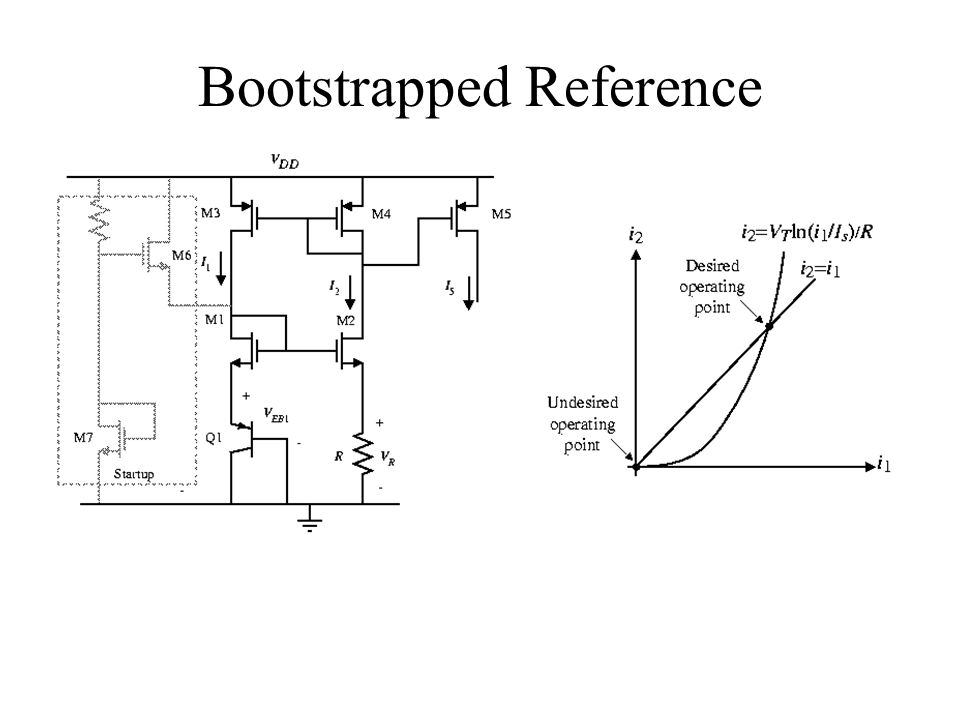
Bootstrapped Reference

29
Startup Circuit

30
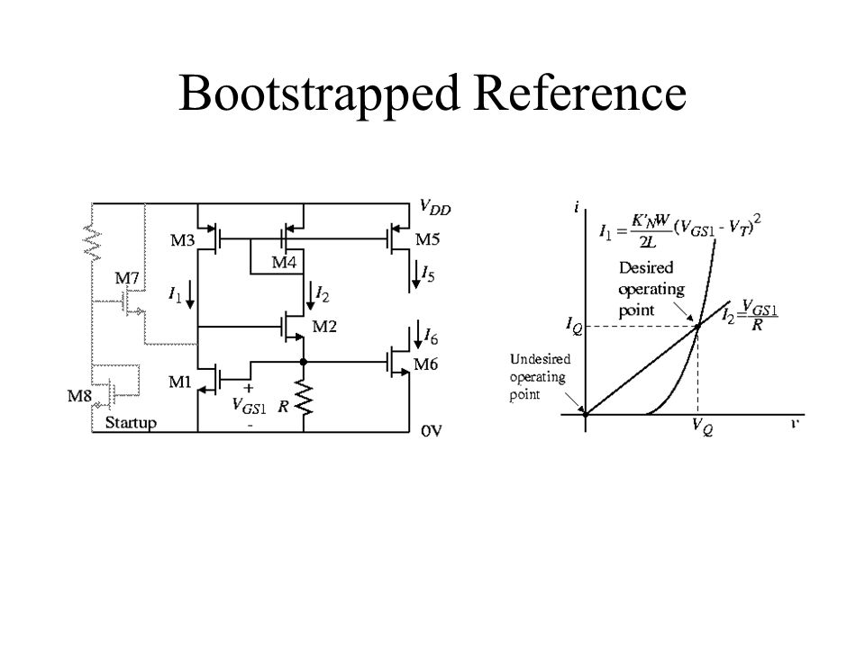
Bootstrapped Reference

32
Startup Circuit

Similar presentations


 Amplifier and Cascode Circuits>")


>")


 Kwangsik Choi.>")


 ENTC 210: Circuit Analysis I Rohit Singhal Lecturer Texas A&M University.>")


 The differential pair with a common-mode input signal vCM. (b) The differential.>")