Download presentation
Presentation is loading. Please wait.

1
Wafer processing - I Clean room environment Semiconductor clean room: - controlled temperature (20ºC), air pressure, humidity (30%) - controlled airbone particulates - controlled vibration - controlled lighting INESC: 250 m 2 Class 10 and 100 clean room 250 m 2 Class 10000 (grey area) Class 100: 0.5 m)/ft 3
, air pressure, humidity (30%) - controlled airbone particulates - controlled vibration - controlled lighting INESC: 250 m 2 Class 10 and 100 clean room 250 m 2 Class (grey area) Class 100: 0.5 m)/ft 3")
3
Wafer processing - II resist coating 1- Vapor priming for improved resist adhesion to substrate - Resist adhesion to Si wafers is poor - Dehydration bake to remove adsorbed water from the surface - surfactant to promote adhesion : HMDS (hexamethyldisilazane) Vapor priming is better than spin coating with a liquid solution because lower contamination ~1 monolayer
 Vapor priming is better than spin coating with a liquid solution because lower contamination ~1 monolayer")
4
2- Spinning resist and soft baking Wafer processing - II resist coating SVG Resist coater and developer track: Track system for spin coating of photoresist (1.2 to 2 m thick) and for development of post-exposed wafers. (cassettes of 25 Si wafers 6 inch) Requirements: Good control of thickness, uniformity, viscosity, particle contamination Typical resist thickness: 0.6-2 m Soft baking: remove solvents and stress and promote adhesion to wafer
 Requirements: Good control of thickness, uniformity, viscosity, particle contamination Typical resist thickness: m Soft baking: remove solvents and stress and promote adhesion to wafer.")
5
Wafer processing - II Coating and developing Exposure (c) 6 inch Si wafers
 6 inch Si wafers")
6
Wafer processing - III exposure Heidelberg Instruments Direct Write Laser Lithography System: Direct write lithography system utilizing a HeCd laser ( =442 nm (g-line) / write lens NA= 0.85) capable of critical dimensions down to 0.8 m. System works with mask designs in GDS2 format. INESC

7
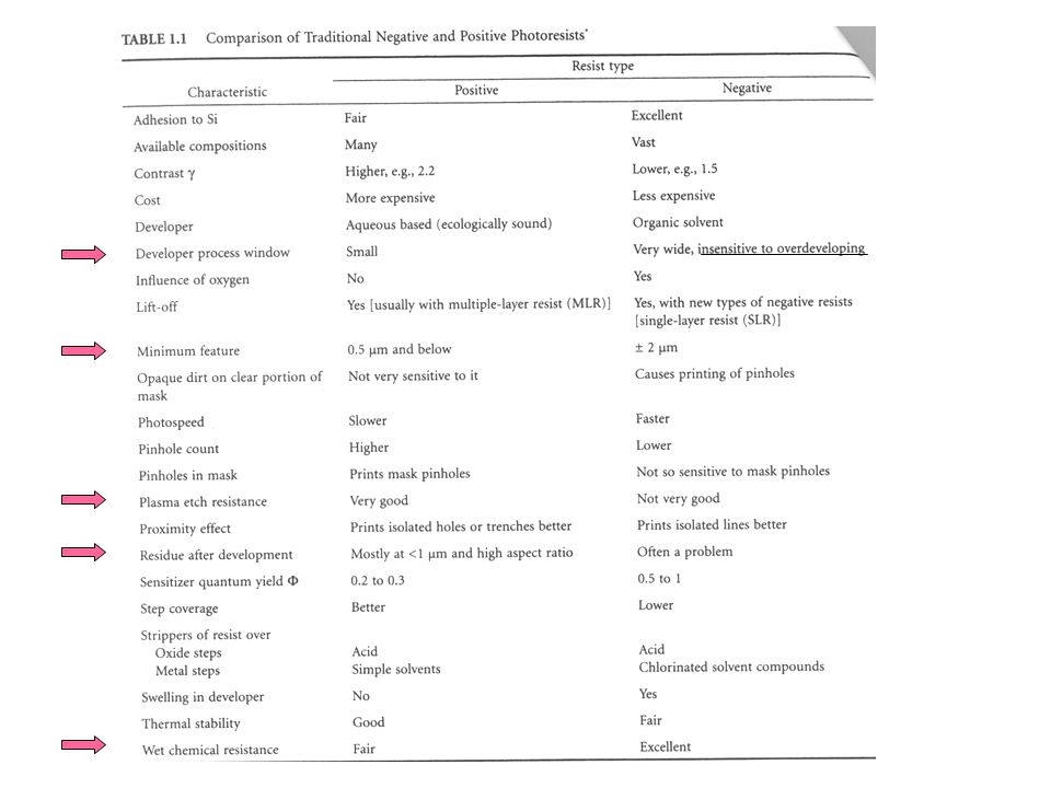
Wafer processing - IV development Positive resists Negative resists (INESC) Solved in the exposed regions Remain in the exposed regions Selective dissolving of resist
 Solved in the exposed regions Remain in the exposed regions Selective dissolving of resist")
9
Resist profiles

Similar presentations


 Grey=Si, Blue=Silicon Dioxide, Red=Photoresist, Purple= Phosphorus.>")


