Download presentation
Presentation is loading. Please wait.

1
HSRA: High-Speed, Hierarchical Synchronous Reconfigurable Array William Tsu, Kip Macy, Atul Joshi, Randy Huang, Norman Walker, Tony Tung, Omid Rowhani, Varghese George, John Wawrzynek, and André DeHon BRASS Project University of California at Berkeley

2
Myth FPGAs inherently run at an order of magnitude lower clock rates than microprocessors.

3
What’s in a Clock Cycle FPGA cycle times are elusive –cycle not defined by architecture –varies almost continuously based on routing –makes timing difficult Processor cycles are well defined –cycle defined by architecture –all operations quantized to this cycle –for all applications => run processor at cycle

4
Defining a Cycle Pick a target clock cycle Define what happens in a clock cycle based on that –how much computation –how much interconnect Assemble computation by combining cycles –...you were paying for the delay anyway...

5
Don’t Believe It! Example: XC4000XL-09 (0.35 m) –Minimum clock low/high 2.3ns 4.6ns cycle –Composing: clock Q 1.5ns interconnect budget 1.5ns logic clock setup 1.6ns 4.6ns Also: Von Herzen FPGA97, XC3100-09 4ns
 –Minimum clock low/high 2.3ns 4.6ns cycle –Composing: clock Q 1.5ns interconnect budget 1.5ns logic clock setup 1.6ns 4.6ns Also: Von Herzen FPGA97, XC 4ns.")
6
Cycle Comparison FPGA cycles comparable to contemporary microprocessors.

7
Outline FPGA cycle times Why low frequency? Architecture and CAD for high frequency HSRA Experiments Assessment

8
Why FPGA designs run slowly? Few designs run at 200+MHz... 1. Limited application/user requirements 2. Cyclic data dependencies 3. Poor tool support 4. Long interconnect delays 5. Pipelining expensive?

9
HSRA High-Speed, Hierarchical Synchronous Reconfigurable Array Attacks architecture and CAD impediments –pipeline the interconnect (4) –balance retiming resources (5) –CAD for auto retiming (3)
 –balance retiming resources (5) –CAD for auto retiming (3)")
10
HSRA Architecture

11
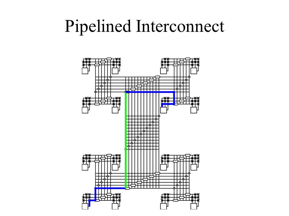
HSRA 5-LUT with 5th input hardwired to neighbor –(can be used 4-input, 2-output LUT w/ some restrictions) Flip-flop bank on inputs for retiming Hierarchical Interconnect Fixed clock cycle (0.4 m = 4ns) Pipelined Interconnect
 Flip-flop bank on inputs for retiming Hierarchical Interconnect Fixed clock cycle (0.4 m = 4ns) Pipelined Interconnect")
13
Input Retiming

14
Balancing Logic Evaluation Cycle (BLB Cascade Timing)
")
15
Hierarchical Interconnect Fat-Tree/Fat-Pyramid inspired network; Geometric bandwidth growth toward root. (Parameterized growth allows exploration/tuning. =>Our recent study suggests p=0.6 good for “random logic”)
.")
16
What Cycle? Data from 0.4 m DRAM Process

17
Area vs. Cycle

18
Flop Experiment #1 Pipeline and retime to single LUT delay per cycle –MCNC benchmarks to 256 4-LUTs –no interconnect accounting –average 1.7 registers/LUT (some circuits 2--7)
")
19
HSRA Retiming One additional twist to retiming task –long, pipelined interconnect need more than one register on paths

20
Accommodating HSRA Interconnect Delays (CAD) Add “logical” buffers to LUT LUT path to match interconnect register requirements Reduces HSRA retiming to existing retiming problem Retime to C=1 as before Buffer chains force enough registers to cover interconnect delays
 Add logical buffers to LUT LUT path to match interconnect register requirements Reduces HSRA retiming to existing retiming problem Retime to C=1 as before Buffer chains force enough registers to cover interconnect delays")
21
Add Interconnect Delays

22
Flop Experiment #2 Pipeline and retime to HSRA cycle –place on HSRA –single LUT or interconnect domain –same MCNC benchmarks –average 4.7 registers/LUT

23
Design Question How deep should we make input retiming register bank? –Most inputs need only one (60%) –Some inputs need very deep (>10) –Average Input depth: 4.7
 –Some inputs need very deep (>10) –Average Input depth: 4.7.")
24
Limit Input Depth Experiment limiting input depths For each output -> input pair –calculate delay –get regs –if (regs-delay) > input_regs allocate retiming buffer(s) to cover regs share among sinks if possible
 > input_regs allocate retiming buffer(s) to cover regs share among sinks if possible")
25
HSRA Input

26
Extra Blocks (limited input depth) AverageWorst Case Benchmark
 AverageWorst Case Benchmark")
27
Input Depth Optimization Real design, fixed input retiming depth –truncate deeper and allocate additional logic blocks

28
HSRA CAD Flow LUT Mapping PartitionPlacement Bitstream Generation Tech. Indep. Optimization Config. Data RTL RoutingRetiming BOOM design generator

29
HSRA Interconnect

30
Mapping => Retiming Exploit technique developed for Systolic Arrays (Leiserson) Retime –find a legal movement of registers to improve circuit performance (area) For HSRA: retime to fully pipeline design –match HSRA cycle –justify / cover interconnect delays
 Retime –find a legal movement of registers to improve circuit performance (area) For HSRA: retime to fully pipeline design –match HSRA cycle –justify / cover interconnect delays")
31
HSRA Retiming Automatic Mapping Attack –pipeline as far as possible –find resulting cycle, C –make C-slow –final retime to distribute C-slow registers

32
Cycle => C-slow

33
Retimed 2-Slow Cycle

34
C-Slow applicable? Available parallelism –solve C identical, independent problems e.g. process packets (blocks) separately e.g. independent regions in images Commutative operators –e.g. max example
 separately e.g. independent regions in images Commutative operators –e.g. max example.")
35
Assessment Cost: –our designs: 1.5 area of no pipelining –plausible ballpark for other designs –w/ 8 deep retiming, 20% BLB overhead –total: 1.8 area Running LUT LUT delay on FPGA –70% overhead for retiming –freq still vary with interconnect Benefits –2--17 higher frequency operation than unpipelined Net Area-Time win + automation/consistency

36
Better way to build Arrays? Can we exploit higher frequency offered? –High throughput, feed-forward –Cycles in flowgraph abundant data level parallelism no data level parallelism –Low throughput tasks structured (e.g. datapaths) unstructured –Data dependent operations similar ops dis-similar ops
 unstructured –Data dependent operations similar ops dis-similar ops.")
37
Better Efficiently use fully spatial design: –feed forward (no cycles, high throughput) –cycles w/ data level parallelism (C-slow) –low throughput datapaths (serialize or swap) –similar data dependent operations (local control, share datapaths) HSRA, clocked interconnect allows –reliable execution at high clock rate –(not achievable with traditional FPGAs)
 –cycles w/ data level parallelism (C-slow) –low throughput datapaths (serialize or swap) –similar data dependent operations (local control, share datapaths) HSRA, clocked interconnect allows –reliable execution at high clock rate –(not achievable with traditional FPGAs)")
38
Remaining Cases Benefit from multicontext as well as high clock rate –cycles, no parallelism –data dependent, dissimilar operations –low throughput, irregular (can’t afford swap?) Single context HSRA and FPGA suffer similarly in these cases HSRA style retiming/pipelining –applicable to multicontext design
 Single context HSRA and FPGA suffer similarly in these cases HSRA style retiming/pipelining –applicable to multicontext design")
39
HSRA Highlights Design achieves 250MHz operation 2M 2 /BLB in subarray –BLB = cascade 5-LUT or 2-output 4-LUT –scales to 6M 2 /BLB for large arrays room for density improvement (not satisfactory) Students in 294-6 (RC Class) demo –full rate filters –FIR –IIR (nice bit-level cycle implementation by Michael Chu)
 Students in (RC Class) demo –full rate filters –FIR –IIR (nice bit-level cycle implementation by Michael Chu)")
40
HSRA Testchip

41
Summary No inherent reasons for FPGAs/RC arrays to run slower than microprocessors Current FPGAs lack architectural and CAD support to reliably achieve high clock rates HSRA demonstrates how to attack problems –retiming balance – interconnect pipelining – automated retiming

42
Berkeley Reconfigurable Architectures Software and Systems (BRASS)
")
Similar presentations

 CTR is a static implementation strategy where each application consists of one.>")


 Day17: November 20, 2000 Time Multiplexing.>")


: Computer Organization Day 21: April 2, 2007 Time Multiplexing.>")


: Computer Organization Day 20: March 28, 2007 Retiming 2: Structures and Balance.>")
 Day8: October 18, 2000 Computing Elements 1: LUTs.>")

: Computer Organization Day 19: March 26, 2007 Retime 1: Transformations.>")
: Computer Organization Day 11: February 14, 2007 Compute 1: LUTs.>")

