Download presentation
Presentation is loading. Please wait.

1
Introduction to Nanoelectronics and Fabrication Dr. Sabar D. Hutagalung School of Materials and Mineral Resources Engineering, Universiti Sains Malaysia, 14300 Nibong Tebal, Penang, Malaysia

2
Nanoscience – Nanoscience – working small, thinking big

3
Nano: From the Greek nanos - meaning "dwarf”, this prefix is used in the metric system to mean 10 -9 or 1/1,000,000,000.

4
What is Nanotechnology? Nanotechnology is the creation of functional materials, devices, and systems through control of matter on the nanometer (1 to 100 nm) length scale and the exploitation of novel properties and phenomena developed at that scale. A scientific and technical revolution has begun that is based upon the ability to systematically organize and manipulate matter on the nanometer length scale.
 length scale and the exploitation of novel properties and phenomena developed at that scale. A scientific and technical revolution has begun that is based upon the ability to systematically organize and manipulate matter on the nanometer length scale..")
5
Is this technology new? In one sense there is nothing new… Whether we knew it or not, every piece of technology has involved the manipulation of atoms at some level. Many existing technologies depend crucially on processes that take place on the nanometer scale. Ex: Photography & Catalysis Nanotechnology, like any other branch of science, is primarily concerned with understanding how nature works.

6
Why is this length scale so important? There are five reasons: The wavelike properties of electrons inside matter are influenced by variations on the nanometer scale. By patterning matter on the nanometer length, it is possible to vary fundamental properties of materials (for instance, melting temperature, magnetization, charge capacity) without changing the chemical composition. The systematic organization of matter on the nanometer length scale is a key feature of biological systems. Nanotechnology promises to allow us to place artificial components and assemblies inside cells, and to make new materials using the self-assembly methods of nature.
 without changing the chemical composition. The systematic organization of matter on the nanometer length scale is a key feature of biological systems. Nanotechnology promises to allow us to place artificial components and assemblies inside cells, and to make new materials using the self-assembly methods of nature..")
7
Nanoscale components have very high surface areas, making them ideal for use in composite materials, reacting systems, drug delivery, and energy storage. The finite size of material entities, as compared to the molecular scale, determine an increase of the relative importance of surface tension and local electromagnetic effects, making nanostructured materials harder and less brittle. The interaction wavelength scales of various external wave phenomena become comparable to the material entity size, making materials suitable for various opto- electronic applications. Why is this length scale so important?

8
How Small We can make the grains? Because of high surface areas conventional powders methods reach their limits at 10 -6 m (1 micron) Smaller particles can be made but special methods are needed!
 Smaller particles can be made but special methods are needed!.")
9
Working at the nanoscale Working in the nanoworld was first proposed by Richard Feynman back in 1959. But it's only true in the last decade. The world of the ultra small, in practical terms, is a distant place. We can't see or touch it. Because, optical microscopes can't provide images of anything smaller than the wavelength of visible light (ie, nothing smaller than 380 nanometres).
..")
10
From “There’s Plenty of Room at the Bottom”, Dec 29, 1959 This image was written using Dip-Pen Nanolithography, and imaged using lateral force microscopy mode of an atomic force microscope.

11
What is Nanoelectronics Nanoelectronic device? A very small devices to ovecome limits on scalability Examples: Single-Electron Transistors controlled electron tunneling to amplify current Resonance Tunneling Device quantum device use to control current

12
Problem of Making More Powerful Chips The number of transistors on a chip will approximately double every 18 to 24 months (Moore’s Law). This law has given chip designers greater incentives to incorporate new features on silicon.

13
Problem of Making More Powerful Chips Moore's Law works largely through shrinking transistors, the circuits that carry electrical signals. By shrinking transistors, designers can squeeze more transistors into a chip.

14
Problem of Making More Powerful Chips However, more transistors means more electricity and heat compressed into a smaller space. Furthermore, smaller chips increase performance but also create the problem of complexity.

15
Problem of Making More Powerful Chips A basic MOSFET Band diagram when on

16
Problem of Making More Powerful Chips Quantum and coherence effects, high electric fields creating avalanche dielectric breakdowns, heat dissipation problems in closely packed structures as well as the non- uniformity of dopant atoms and the relevance of single atom defects are all roadblocks along the current road of miniaturization.

17
Problem of Making More Powerful Chips Problem 1: Carrier mobility decreases as channel length decrease and vertical electric fields increase.

18
Problem of Making More Powerful Chips Problem 2: Tunneling through gate oxide (off state current). E ox

19
Problem of Making More Powerful Chips Problem 3: Wattage/Area increases as density increases

20
Single-Electron Transistors (SETs) To solve these problem, the single-electron tunneling transistor - a device that exploits the quantum effect of tunneling to control and measure the movement of single electrons was developed. Experiments have shown that charge does not flow continuously in these devices but in a quantized way. Fig. A single-electron transistor

21
Single-Electron Transistors (SETs) SET consists of a gate electrode that electrostaticaly influences electrons traveling between the source and drain electrodes. The electrons in the SET need to cross two tunnel junctions that form an isolated conducting electrode called the island. Fig. A single-electron transistor

22
Single-Electron Transistors (SETs) Electrons passing through the island charge and discharge it, and the relative energies of systems containing 0 or 1 extra electrons depends on the gate voltage. The key point is that charge passes through the island in quantized units. Fig. A single-electron transistor

23
Single-Electron Transistors (SETs) For an electron to hop onto the island, its energy must equal the Coulomb energy, e 2 /2C. When both the gate and bias voltages are zero, electrons do not have enough energy to enter the island and current does not flow. Fig. A single-electron transistor

24
Single-Electron Transistors (SETs) As the bias voltage between the source and drain is increased, an electron can pass through the island when the energy in the system reaches the Coulomb energy. This effect is known as the Coulomb blockade, and the critical voltage needed to transfer an electron onto the island, equal to e/2C, is called the Coulomb gap voltage. Fig. A single-electron transistor

25
Here n 1 and n 2 are the number of electrons passed through the tunnel barriers 1 and 2, respectively, so that n = n 1 - n 2, while the total island capacitance, C ∑, is now a sum of C G, C 1, C 2, and whatever stray capacitance the island may have. Left: Equivalent circuit of an SET Center: Energy states of an SET. Top Coulomb blockade regime, bottom transfer regime by application of V G =e/2C G Right: I-V characteristic for two different gate voltages. Solid line V G = e/2C G, dashed line V G =0

26
The Coulomb blockade is a single-electron phenomenon, which originates in the discrete nature of electric charge that can be transferred from a conducting island connected to electron reservoirs through thin barriers. The CB allows a precise control of small number of electrons, with important application in switching devices with low power dissipation and a corresponding increased level of circuit integration. Coulomb Blockade Single-electron devices based on the Coulomb blockade.

27
DOT I-V curve controlled by gate voltage, showing region of QB Tunneling & Q Blockade in SET Q transport by single-electron tunneling, but essentially suppressed by Coulomb charging energy: E c > k b T ( E c = e 2 /2C Σ ) Tunneling resistance, R t > R k (Junction resistance, R k = h/e 2 = 25.8 K )
 Tunneling resistance, R t > R k (Junction resistance, R k = h/e 2 = 25.8 K )")
28
Silicon SET

29
Silicon nanowire transistors

30
Enhanced Channel Modulation in Dual-Gated Silicon Nanowire Transistors Nano Letters Vol. 5, 2005, 2519-2523

31
(a)Schematic of a NW FET, and (inset) FE-SEM image of a GaN NW FET. (b)Gate-dependent I–V sd data recorded on a 17.6 nm diameter GaN NW. The gate voltages for each I–V sd curve are indicated; (c)I–V g data recorded for values of V sd. (Inset) Conductance, G, vs gate voltage C.N.R. Rao et al. / Progress in Solid State Chemistry 31 (2003) 5–147.
Gate-dependent I–V sd data recorded on a 17.6 nm diameter GaN NW. The gate voltages for each I–V sd curve are indicated; (c)I–V g data recorded for values of V sd. (Inset) Conductance, G, vs gate voltage C.N.R. Rao et al. / Progress in Solid State Chemistry 31 (2003) 5–147..")
32
ZnO nanorod FETs Park et al., APL, 85 (2004) 5052-5054 (a)Schematic side view and (b)field-emission scanning electron microscopy (FESEM) image of a ZnO nanorod FET device. ZnO nanorod FETs with backgate geometry were fabricated on SiO 2 /Si by deposition of Au/Ti metal electrodes for source-drain contacts on nanorod ends.

33
(a) Typical I sd –V sd characteristic curves as a function of V g for ZnO nanorod FETs. The linear and symmetric I sd –V sd curves were obtained under different V g, indicating the low resistant ohmic contact formation between ZnO and Ti metal layers. (b) I sd –V g curves of ZnO nanorod FETs show that the devices operate in an n-channel depletion mode with g m of ~140 nS for V sd = 1.0 V. Park et al., APL, 85 (2004) 5052-5054
 I sd –V g curves of ZnO nanorod FETs show that the devices operate in an n-channel depletion mode with g m of ~140 nS for V sd = 1.0 V. Park et al., APL, 85 (2004)")
34
FET fabricated based on In 2 O 3 nanowires: (a) I–V curves recorded on an In 2 O 3 nanowire of 10 nm diameter, (b) I–V g data of the same device at V ds = 10 mV. Inset shows the SEM image of the nanowire between the source and drain electrodes.

35
Direct Integration of Metal Oxide Nanowire in Vertical Field-Effect Transistor Nano Letters Vol. 4, 2004

36
Carbon Nanotube Transistor

37
Nanoelectronic Fabrication

38
Nanofabrication Top-down Approach Bottom-up Approach

39
Top-down techniques take a bulk material, machine it, modify it into the desired shape and product classic example is manufacturing of integrated circuits using a sequence of steps sush as crystal growth, lithography, deposition, etching, CMP, ion implantation… (Microelectronic/Nanoelectronics Fabrication Approach) Bottom-up techniques build something from basic materials assembling from the atoms/molecules up not completely proven in manufacturing yet Examples: Self-assembly Sol-gel technology Deposition (old but is used to obtain nanotubes, nanowires, nanoscale films…) Manipulators (AFM, STM,….) Top-down vs Bottom-up
 Bottom-up techniques build something from basic materials assembling from the atoms/molecules up not completely proven in manufacturing yet Examples: Self-assembly Sol-gel technology Deposition (old but is used to obtain nanotubes, nanowires, nanoscale films…) Manipulators (AFM, STM,….) Top-down vs Bottom-up")
40
Top-down From large items to smaller ones. The most common method are electron beam lithography (EBL) and scanning probe lithography (SPL). The approach involves molding or etching materials into smaller components. Making IC? Starting with a thin sheet Si wafer, cleaned, coated, preferentially etched using highly focused optics in as many as 100 separate operations before the final IC is complete.
 and scanning probe lithography (SPL). The approach involves molding or etching materials into smaller components. Making IC. Starting with a thin sheet Si wafer, cleaned, coated, preferentially etched using highly focused optics in as many as 100 separate operations before the final IC is complete..")
41
Bottom-up A general approach going from small items to bigger ones. Building larger, more complex objects by integration of smaller building blocks or components. The sketch shows the essence of bottom-up manufacturing. Self-assembly from the gaseous phase. Two principle vapor-phase technologies that are useful and widely practiced: molecular beam epitaxy (MBE) and vapor-deposition (PVD, CVD).
 and vapor-deposition (PVD, CVD)..")
42
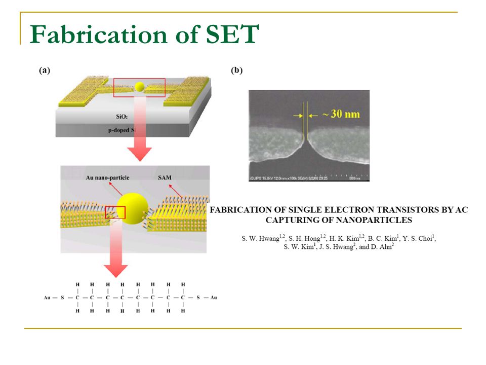
Fabrication of SET SET with a nano particle SET with a nano particle connected by SWCNs

43
FIG. (a) Sketch of the SOI nanowire: a metallic top gate is separated from the SiNW by a 55 nm silicon oxide. (b) SEM micrograph of the nanowire with a width below 10 nm and a length of 500 nm. PHYSICAL REVIEW B 68, 075311 (2003) Fabrication of SET
 Sketch of the SOI nanowire: a metallic top gate is separated from the SiNW by a 55 nm silicon oxide. (b) SEM micrograph of the nanowire with a width below 10 nm and a length of 500 nm. PHYSICAL REVIEW B 68, (2003) Fabrication of SET.")
46
Fig. Patterning of SiNWs. (A) Overview and (B) zoomed in image of patterned lines of vertical SiNWs grown from lines of single nanoparticle catalysts deposited onto a Si substrate. (C) A crosssection SEM image of nanowires that were positionally aligned into lines. Non-Lithographic Positional Control of SiNWs The scale bar in images (A), (B), and (C) correspond to 100 µm, 1 µm, and 1µm. Goldberger, Hochbaum, Fan, and Yang, Nano Letters, 6 (2006) 973 - 977
 Overview and (B) zoomed in image of patterned lines of vertical SiNWs grown from lines of single nanoparticle catalysts deposited onto a Si substrate. (C) A crosssection SEM image of nanowires that were positionally aligned into lines. Non-Lithographic Positional Control of SiNWs The scale bar in images (A), (B), and (C) correspond to 100 µm, 1 µm, and 1µm. Goldberger, Hochbaum, Fan, and Yang, Nano Letters, 6 (2006)")
47
Blue corresponds to the Si substrate and the SiNWs channel, grey is SiO 2 dielectric material, and red corresponds to the Cr gate metal. Vertically Integrated Nanowire Field Effect Transistors (VINFET) Fig. Si VINFET fabrication. (A) SiNWs are grown vertically from a Si(111) substrate. (B) Thermal oxidation of the Si nanowire is used to form the gate dielectric. (C) The Cr gate material is then sputtered onto the nanowires to achieve a conformal coating. Goldberger, Hochbaum, Fan, and Yang, Nano Letters, 6 (2006) 973 - 977
 Fig. Si VINFET fabrication. (A) SiNWs are grown vertically from a Si(111) substrate. (B) Thermal oxidation of the Si nanowire is used to form the gate dielectric. (C) The Cr gate material is then sputtered onto the nanowires to achieve a conformal coating. Goldberger, Hochbaum, Fan, and Yang, Nano Letters, 6 (2006)")
48
Fig. Si VINFET fabrication. (A) Conformal LPCVD oxide is deposited around the nanowire. (B) The Cr-coated nanowire tips are exposed via chemomechanical polishing and plasma etching of the SiO 2 dielectric. (C) The Cr gate material is etched-backed using a Cr photomask etchant. (D) An SEM image taken after the SiO 2 deposition. (E) An SEM image showing the exposed Cr-coated tips. (F) an SEM image of the device after the Cr etch back procedure. Goldberger, Hochbaum, Fan, and Yang, Nano Letters, 6 (2006) 973 - 977
 The Cr-coated nanowire tips are exposed via chemomechanical polishing and plasma etching of the SiO 2 dielectric. (C) The Cr gate material is etched-backed using a Cr photomask etchant. (D) An SEM image taken after the SiO 2 deposition. (E) An SEM image showing the exposed Cr-coated tips. (F) an SEM image of the device after the Cr etch back procedure. Goldberger, Hochbaum, Fan, and Yang, Nano Letters, 6 (2006)")
49
Fig. Si VINFET fabrication. (A) Another layer of LPCVD SiO 2 is deposited onto the nanowire. (B) The nanowire tips are exposed via plasma etching of the SiO 2 dielectric. (C) Ni / Pt contacts are sputtered onto the sample to form the drain electrode. Cr gate material is then sputtered onto the nanowires to achieve a conformal coating. Yellow corresponds to the Ni drain material. Goldberger, Hochbaum, Fan, and Yang, Nano Letters, 6 (2006) 973 - 977
 The nanowire tips are exposed via plasma etching of the SiO 2 dielectric. (C) Ni / Pt contacts are sputtered onto the sample to form the drain electrode. Cr gate material is then sputtered onto the nanowires to achieve a conformal coating. Yellow corresponds to the Ni drain material. Goldberger, Hochbaum, Fan, and Yang, Nano Letters, 6 (2006)")
50
In the case for our system (p-type nanowires) with a Cr gate electrode, the threshold voltage (V t ); Where V FB is the flatband voltage, N A is the acceptor concentration in Si, C is the oxide capacitance, ε s is the oxide permittivity, and φ s is the surface potential. Since the onset of accumulation for an metal-oxide-semiconductor system occurs when the surface potential is zero, the threshold voltage is equal to the flatband potential. V FB can be deduced by the following equation; Where Φ M is the gate work function, χ is the electron affinity of Si, and E g is the band gap of silicon. Φ F is given by the formula; Threshold Voltage Analysis Goldberger, Hochbaum, Fan, and Yang, Nano Letters, 6 (2006) 973 - 977
")
51
Where n i is the intrinsic carrier concentration in Si. More accurate analyses of the influence of carrier concentration on threshold voltage at these small length scales can be derived using drift-diffusion simulations. Threshold Voltage Analysis Goldberger, Hochbaum, Fan, and Yang, Nano Letters, 6 (2006) 973 - 977
")
52
(B) I ds vs V gs with V ds ranging from -1.0 V to -0.2 V in 0.2 V steps, from top to bottom, respectively, measured from a device with 48 nanowires in parallel. (C) TEM image of a 6.5 nm SiNW, obtained from the device used in (A). Scale bar is 100 nm. A typical device has a ~6-7 nm SiNWs diameter, surrounded by a ~30- 35 nm thick shell of SiO 2, and a Cr metal gate length of ~300-350 nm. Fig. Ultra-thin body VINFET. (A) Cross-sectional SEM image. The scale bar is 200 nm. Blue is Si source, grey SiO 2 dielectric, red the gate material, and yellow the drain metal. The SiNW is not colored, due to the inability of resolving this feature via SEM. The Cr coverage on the front of the wire was likely stripped during cleavage. Goldberger, Hochbaum, Fan, and Yang, Nano Letters, 6 (2006) 973 - 977
 TEM image of a 6.5 nm SiNW, obtained from the device used in (A). Scale bar is 100 nm. A typical device has a ~6-7 nm SiNWs diameter, surrounded by a ~ nm thick shell of SiO 2, and a Cr metal gate length of ~ nm. Fig. Ultra-thin body VINFET. (A) Cross-sectional SEM image. The scale bar is 200 nm. Blue is Si source, grey SiO 2 dielectric, red the gate material, and yellow the drain metal. The SiNW is not colored, due to the inability of resolving this feature via SEM. The Cr coverage on the front of the wire was likely stripped during cleavage. Goldberger, Hochbaum, Fan, and Yang, Nano Letters, 6 (2006)")
53
Fabrication Approaches to Nanowires Devices Removing the nanorods/nanowires from the initial growth susbtrate is by sonification in a solvent such ethano. Fig. shows ZnO nanorods after growth on the Si substrate (left) and after 5 min sonification in ethanol (right). The acoustic energy supplied to the solvent is enough to dislodge a large fraction of the nanorods and disperse them into the solution. It was found that >90% of the nanorods could be harvested in this manner. Mater. Sci. Eng. R 47 (2004) 1–47
 and after 5 min sonification in ethanol (right). The acoustic energy supplied to the solvent is enough to dislodge a large fraction of the nanorods and disperse them into the solution. It was found that >90% of the nanorods could be harvested in this manner. Mater. Sci. Eng. R 47 (2004) 1–47.")
54
Transfer of the nanorods from the ethanol solution to a new substrate is by dispersing the solution onto the new substrate, followed by evaporation of the ethanol. The advantage of this approach is simplicity but the main drawback is the random nature of where the nanorods are placed.

55
The approach is to initially prepare an SiO 2 -coated Si wafer and etch alignment marks into the SiO 2. Once the NWs are on this new substrate, a mask design for the particular device being fabricated using software on an e-beam writer and then transferred lithographically so that the ends of the NWs are covered by Ohmic contact pads. The approach

56
Fig. SEM micrographs of structure for transport measurements of ZnO nanowires (top) and close-up of central region (bottom). Fig. Schematic of ZnO nanowire depletion- mode FET.
 and close-up of central region (bottom). Fig. Schematic of ZnO nanowire depletion- mode FET..")
57
SET Fabrication Using EBL Wafer Cutting (sample size 15 mm X 15 mm) Wafer Cleaning (Standard Cleaning 1) Substrate Heating Up (200ºC, 30 minutes) Spin Coating (3000 rpm spin speed, 30 seconds) Pre-bake Hotplate (90ºC, 2 minutes) E-beam Exposure (Exposure e-beam doses variation) Development (ma-D 532, 25 seconds) Rinse in Stopper (De-Water, 5 minutes) Uda Hashim et al, UniMAP
 Wafer Cleaning (Standard Cleaning 1) Substrate Heating Up (200ºC, 30 minutes) Spin Coating (3000 rpm spin speed, 30 seconds) Pre-bake Hotplate (90ºC, 2 minutes) E-beam Exposure (Exposure e-beam doses variation) Development (ma-D 532, 25 seconds) Rinse in Stopper (De-Water, 5 minutes) Uda Hashim et al, UniMAP")
58
Source-Drain & Quantum Dot Design Mask SET Mask design schematic SET Mask Design using GDSII Editor Uda Hashim et al, UniMAP

59
Nanodevices Patterned Using SPL (Scanning Probe Lithography)
")
60
Tunneling Current Metal Tip Sample e - cloud Scanning probe microscope (SPM): from STM to AFM SPM was originated from the scanning tunneling microscopy (STM). SPM is a relatively new family of microscope that can measure surface morphology down to atomic resolution, 3D imaging, and make nanopatterns (line or dot arrays). STM uses the tunneling current flowing between tip and sample to map the topography. STM is limited to conductive samples.
. STM uses the tunneling current flowing between tip and sample to map the topography. STM is limited to conductive samples..")
61
Atomic Force Microscopy (AFM) extended the applications of SPM For conductive & non-conductive samples, even in solutions. AFM measures the attractive or repulsive forces between the tip and sample. Many surface/interface properties (mechanical, magnetic, electric, optical, thermal, chemical properties) can be measured using AFM. AFM also used for fabrication of various nanostructures patterns (AFM-based nanolithography). Scanning probe microscope (SPM): from STM to AFM
 can be measured using AFM. AFM also used for fabrication of various nanostructures patterns (AFM-based nanolithography). Scanning probe microscope (SPM): from STM to AFM.")
62
10 mm 10 um 10 nm 10 um10 mm X,Y Resolution Z Resolution SEM Optical Microscope 10 pm SPM TEM Comparison of SPM and other Microscope 0.2 nm 800 um 15 um

63
Semi- conductor SiGaAs PolymerPlasticRubberStoragedeviceHDCD・DVDMemoryFerroelectric device deviceMemory Thin film BiotechnologyProteinCellDNAInorganicGlassCeramicsMetal Ra ・ Particle & grain analysis ・ Pitch & height measurement Ra ・ Particle & grain analysis ・ Pitch & height measurement Topography VE ・ Friction ・ Adhesion ・ Hardness ( Nano-indentation ) Mechanical Leak Current ・ Polarization ・ Dielectric constant ・ Surface Potential Electric Magnetic Force ・ Magnetic Domain & Flux Magnetic Fluorescence ・ Spectrum ・ Optical Transition ・ Optical Record Optical Lithography ・ Manipulation ・ oxidization ・ Scratch Processing Applications of Multi-function SPM
 Mechanical Leak Current ・ Polarization ・ Dielectric constant ・ Surface Potential Electric Magnetic Force ・ Magnetic Domain & Flux Magnetic Fluorescence ・ Spectrum ・ Optical Transition ・ Optical Record Optical Lithography ・ Manipulation ・ oxidization ・ Scratch Processing Applications of Multi-function SPM")
64
Scanning Probe Lithograpy (SPL) One of the most methods is local anodic oxidation (LAO) by AFM where the application of a +ve voltage to the surface with respect to the tip in humidity atmosphere. By controlling the certain condition between the AFM tip and the sample, desired nanopatterns can be created.

65
Experimental Method Silicon wafer (n-type 100) Silicon wafer (n-type 100) NanoPatterning (by AFM) NanoPatterning RCA Cleaning (RCA 1 & RCA 2) RCA Cleaning (RCA 1 & RCA 2) Passivated (5 % HF 10 s) Passivated Surface Analysis (by AFM) Surface Analysis (by AFM) SPI3800N Series with SPA-300HV NanoNavi (vector & raster scan), conductive AFM tip (coated Rh, TIP 20 – 30 nm)
 Silicon wafer (n-type 100) NanoPatterning (by AFM) NanoPatterning RCA Cleaning (RCA 1 & RCA 2) RCA Cleaning (RCA 1 & RCA 2) Passivated (5 % HF 10 s) Passivated Surface Analysis (by AFM) Surface Analysis (by AFM) SPI3800N Series with SPA-300HV NanoNavi (vector & raster scan), conductive AFM tip (coated Rh, TIP 20 – 30 nm)")
66
Vector Scan BeforeAfter AFM Lithography (Si wafer) by electrolyte oxidation 0.2μ m Scan Electrolyte Oxidation Cantilever
 by electrolyte oxidation 0.2μ m Scan Electrolyte Oxidation Cantilever")
67
Raster Scan - Fine fabrication by Raster Scan - Nano dots on Si wafer sample ( D: 60n m) Symbol image by Raster scan By : Nano function Project team NITS Nano Tech. depart. BMP file of design After fabrication (20 μ m □ ) Recall BMP file
 Recall BMP file.")
68
Vector Scan 、 Raster Scan - Influence of absorbed water layer Fabrication by Raster scan Apply 5V Voltage to 1μm area Measurement area 2μm Air Vacuum ( 4×10 -6 Torr ) 200nm
 200nm")
69
OXIDIZED LINE SCRATCH LINE SILICON WAFER OXIDIZED DOT Scratch and Oxide Line

70
Single dot, double dots, and triple dots patterned on silicon surface at -8V tip bias voltage with different oxidation time. 3 ms5 ms 8 ms1 ms

71
Dot Oxide Array on Si (100) wafer ( h 10 nm and w 200 nm )
 wafer ( h 10 nm and w 200 nm )")
72
Oxide Dot Array (Surface Profile)
")
73
Line Oxide

74
Line Oxide (With Profile)
")
75
LAO Mechanism The oxides grow on substrate by the application of a voltage between a conductive tip (cathode) and a substrate (anode). Water molecules adsorbed on a substrate dissociates into fragments (e.g. H +, OH -, and O 2- ) and acts as electrolyte. Schematic diagram of local- anodic-oxidation (LAO) process performed by AFM. Cervenka et al., Appl. Surf. Sci., 253 (2006) 2373. T.-H. Fang, Microelectronics Journal, 35 (2004) 70.
 and acts as electrolyte. Schematic diagram of local- anodic-oxidation (LAO) process performed by AFM. Cervenka et al., Appl. Surf. Sci., 253 (2006) T.-H. Fang, Microelectronics Journal, 35 (2004) 70..")
76
LAO Mechanism At the Si/SiO 2 interface, OH - react with holes h + as follow: Si + 4h + + 2OH − SiO 2 + 2H + The proton concentration increases after long pulse times, with the H + + OH − H 2 O neutralization reaction. Schematic diagram of local- anodic-oxidation (LAO) process performed by AFM. Cervenka et al., Appl. Surf. Sci., 253 (2006) 2373. T.-H. Fang, Microelectronics Journal, 35 (2004) 70.
 process performed by AFM. Cervenka et al., Appl. Surf. Sci., 253 (2006) T.-H. Fang, Microelectronics Journal, 35 (2004) 70..")
77
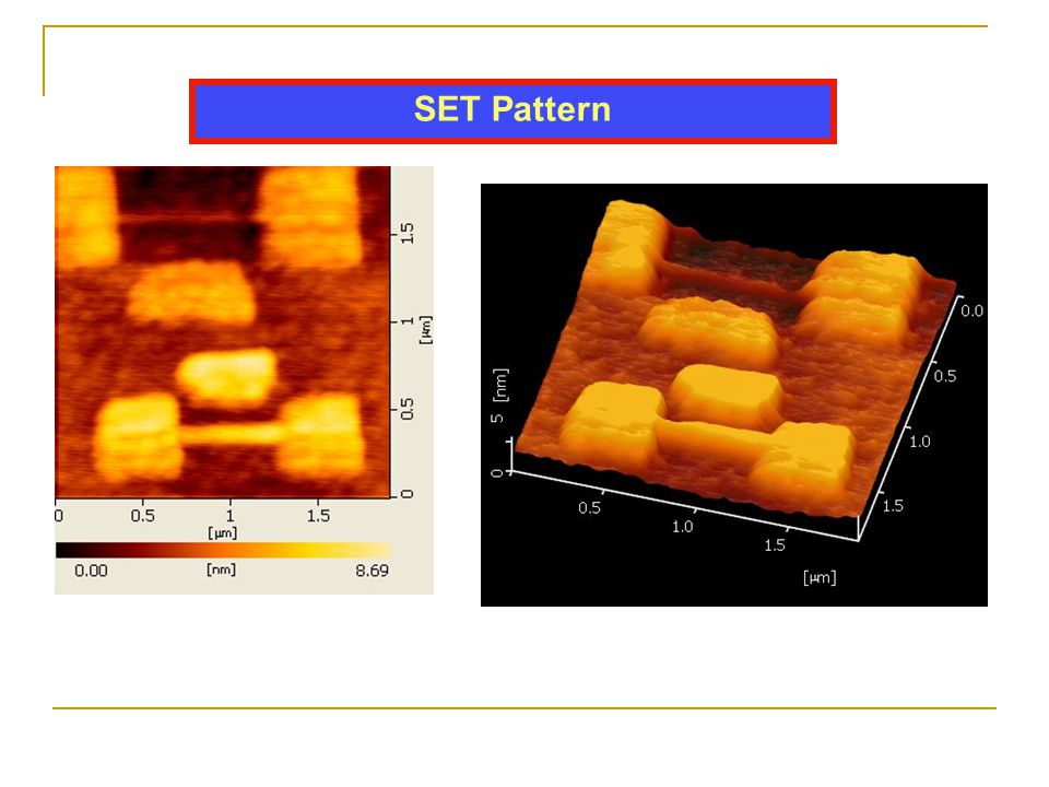
SET Pattern

79
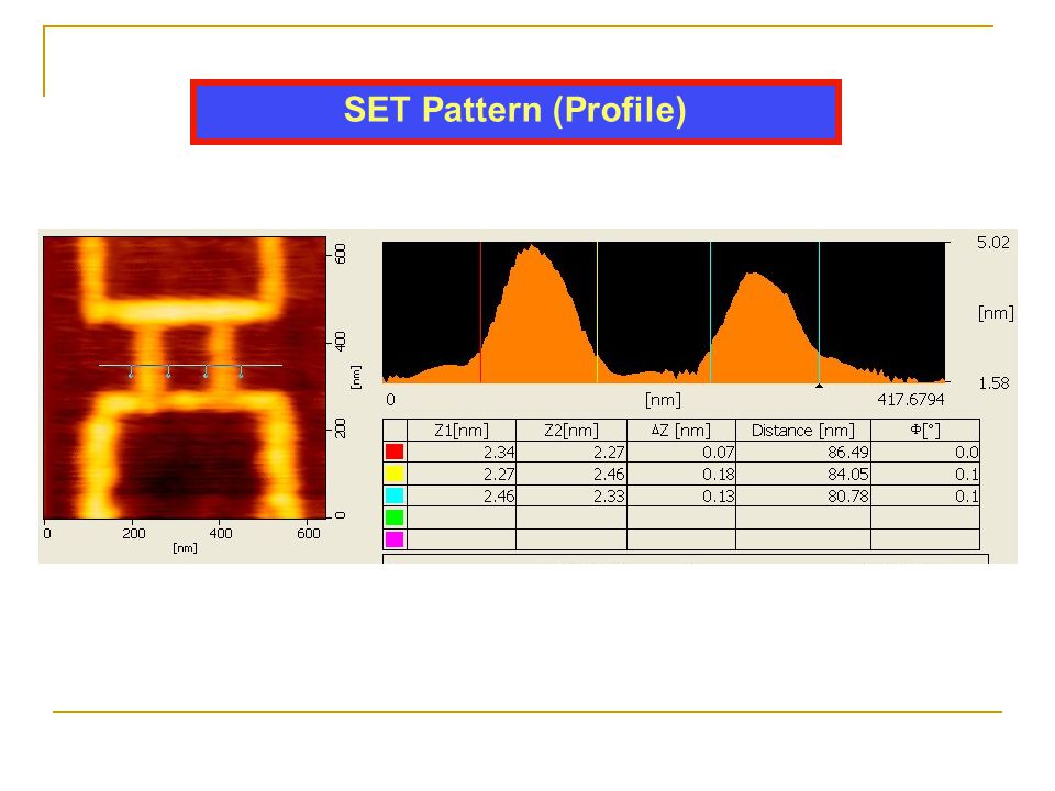
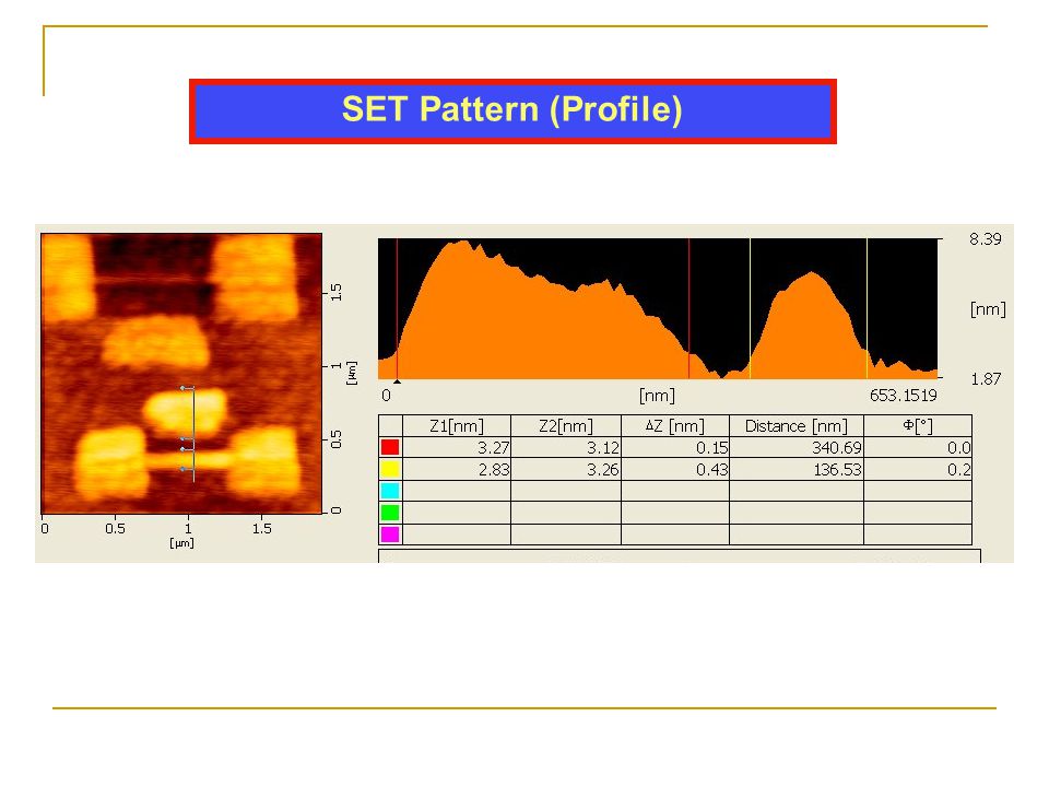
SET Pattern (Profile)
")
82
USM letter Oxide on Si (100) wafer
 wafer")
83
Summary Nanoelectronics is not only about size but also phenomena, mechanism, etc. Nanoelctronics is a wide open field with vast potential for breakthroughs coming from fundamental research. Some of the major issues that need to be addressed are: Understand nanoscale transport (theory & experimental). Develop/understand self-assembly techniques to do conventional things cheaper. Find new ways of doing electronics and find ways of implementing them (e.g. quantum computing; hybrid Si- biological systems; cellular automata).
. Develop/understand self-assembly techniques to do conventional things cheaper. Find new ways of doing electronics and find ways of implementing them (e.g. quantum computing; hybrid Si- biological systems; cellular automata)..")
Similar presentations


>")


 have displayed exceptional electrical properties superior to the traditional MOSFET. Most of these.>")


>")


 as chemical or biological sensors is.>")
>")
>")
