Download presentation
Presentation is loading. Please wait.

1
Embedded Systems Design: A Unified Hardware/Software Introduction 1 Chapter 3 General-Purpose Processors: Software ECE 4330 Embedded System Design

2
2 Introduction General-Purpose Processor –Processor designed for a variety of computation tasks –Low unit cost, in part because manufacturer spreads NRE over large numbers of units Motorola sold half a billion 68HC05 microcontrollers in 1996 alone –Carefully designed since higher NRE is acceptable Can yield good performance, size and power –Low NRE cost, short time-to-market/prototype, high flexibility User just writes software; no processor design –a.k.a. “microprocessor” – “micro” used when they were implemented on one or a few chips rather than entire rooms

3
ECE 4330 Embedded System Design 3 Basic Architecture Control unit and datapath –Note similarity to single-purpose processor Key differences –Datapath is general –Control unit doesn’t store the algorithm – the algorithm is “programmed” into the memory Processor Control unitDatapath ALU Registers IRPC Controller Memory I/O Control /Status

4
ECE 4330 Embedded System Design 4 Datapath Operations Load –Read memory location into register ALU operation –Input certain registers through ALU, store back in register Store –Write register to memory location Processor Control unitDatapath ALU Registers IRPC Controller Memory I/O Control /Status 10... 10 +1 11

5
ECE 4330 Embedded System Design 5 Control Unit Control unit: configures the datapath operations –Sequence of desired operations (“instructions”) stored in memory – “program” Instruction cycle – broken into several sub-operations, each one clock cycle, e.g.: –Fetch: Get next instruction into IR –Decode: Determine what the instruction means –Fetch operands: Move data from memory to datapath register –Execute: Move data through the ALU –Store results: Write data from register to memory Processor Control unitDatapath ALU Registers IRPC Controller Memory I/O Control /Status 10... load R0, M[500] 500 501 100 inc R1, R0 101 store M[501], R1 102 R0R1

6
ECE 4330 Embedded System Design 6 Control Unit Sub-Operations Fetch –Get next instruction into IR –PC: program counter, always points to next instruction –IR: holds the fetched instruction Processor Control unitDatapath ALU Registers IRPC Controller Memory I/O Control /Status 10... load R0, M[500] 500 501 100 inc R1, R0 101 store M[501], R1 102 R0R1100 load R0, M[500]

7
ECE 4330 Embedded System Design 7 Control Unit Sub-Operations Decode –Determine what the instruction means Processor Control unitDatapath ALU Registers IRPC Controller Memory I/O Control /Status 10... load R0, M[500] 500 501 100 inc R1, R0 101 store M[501], R1 102 R0R1100 load R0, M[500]

8
ECE 4330 Embedded System Design 8 Control Unit Sub-Operations Fetch operands –Move data from memory to datapath register Processor Control unitDatapath ALU Registers IRPC Controller Memory I/O Control /Status 10... load R0, M[500] 500 501 100 inc R1, R0 101 store M[501], R1 102 R0R1100 load R0, M[500] 10

9
ECE 4330 Embedded System Design 9 Control Unit Sub-Operations Execute –Move data through the ALU –This particular instruction does nothing during this sub-operation Processor Control unitDatapath ALU Registers IRPC Controller Memory I/O Control /Status 10... load R0, M[500] 500 501 100 inc R1, R0 101 store M[501], R1 102 R0R1100 load R0, M[500] 10

10
ECE 4330 Embedded System Design 10 Control Unit Sub-Operations Store results –Write data from register to memory –This particular instruction does nothing during this sub-operation Processor Control unitDatapath ALU Registers IRPC Controller Memory I/O Control /Status 10... load R0, M[500] 500 501 100 inc R1, R0 101 store M[501], R1 102 R0R1100 load R0, M[500] 10

11
ECE 4330 Embedded System Design 11 Instruction Cycles Processor Control unitDatapath ALU Registers IRPC Controller Memory I/O Control /Status 10... load R0, M[500] 500 501 100 inc R1, R0 101 store M[501], R1 102 R0R1 PC= 100 10 Fetch ops Exec. Store results clk Fetch load R0, M[500] Decode 100

12
ECE 4330 Embedded System Design 12 Instruction Cycles Processor Control unitDatapath ALU Registers IRPC Controller Memory I/O Control /Status 10... load R0, M[500] 500 501 100 inc R1, R0 101 store M[501], R1 102 R0R1 10 PC= 100 FetchDecode Fetch ops Exec. Store results clk PC= 101 inc R1, R0 Fetch Fetch ops +1 11 Exec. Store results clk 101 Decode

13
ECE 4330 Embedded System Design 13 Instruction Cycles Processor Control unitDatapath ALU Registers IRPC Controller Memory I/O Control /Status 10... load R0, M[500] 500 501 100 inc R1, R0 101 store M[501], R1 102 R0R1 1110 PC= 100 FetchDecode Fetch ops Exec. Store results clk PC= 101 FetchDecode Fetch ops Exec. Store results clk PC= 102 store M[501], R1 Fetch Fetch ops Exec. 11 Store results clk Decode 102

14
ECE 4330 Embedded System Design 14 Architectural Considerations N-bit processor –N-bit ALU, registers, buses, memory data interface –Embedded: 8-bit, 16- bit, 32-bit common –Desktop/servers: 32- bit, even 64 PC size determines address space Processor Control unitDatapath ALU Registers IRPC Controller Memory I/O Control /Status

15
ECE 4330 Embedded System Design 15 Architectural Considerations Clock frequency –Inverse of clock period –Must be longer than longest register to register delay in entire processor –Memory access is often the longest Processor Control unitDatapath ALU Registers IRPC Controller Memory I/O Control /Status

16
ECE 4330 Embedded System Design 16 Pipelining: Increasing Instruction Throughput 12345678 12345678 12345678 12345678 Fetch-instr. Decode Fetch ops. Execute Store res. 12345678 12345678 12345678 12345678 12345678 Wash Dry Time Non-pipelinedPipelined Time Pipelined pipelined instruction execution non-pipelined dish cleaningpipelined dish cleaning Instruction 1

17
ECE 4330 Embedded System Design 17 Superscalar and VLIW Architectures Performance can be improved by: –Faster clock (but there’s a limit) –Pipelining: slice up instruction into stages, overlap stages –Multiple ALUs to support more than one instruction stream Superscalar –Scalar: non-vector operations –Fetches instructions in batches, executes as many as possible May require extensive hardware to detect independent instructions –VLIW: each word in memory has multiple independent instructions Relies on the compiler to detect and schedule instructions Currently growing in popularity
 –Pipelining: slice up instruction into stages, overlap stages –Multiple ALUs to support more than one instruction stream Superscalar –Scalar: non-vector operations –Fetches instructions in batches, executes as many as possible May require extensive hardware to detect independent instructions –VLIW: each word in memory has multiple independent instructions Relies on the compiler to detect and schedule instructions Currently growing in popularity")
18
ECE 4330 Embedded System Design 18 Two Memory Architectures Processor Program memory Data memory Processor Memory (program and data) HarvardPrinceton –Fewer memory wires Harvard –Simultaneous program and data memory access
 HarvardPrinceton –Fewer memory wires Harvard –Simultaneous program and data memory access")
19
ECE 4330 Embedded System Design 19 Cache Memory Memory access may be slow Cache is small but fast memory close to processor –Holds copy of part of memory –Hits and misses Processor Memory Cache Fast/expensive technology, usually on the same chip Slower/cheaper technology, usually on a different chip

20
ECE 4330 Embedded System Design 20 Programmer’s View Programmer doesn’t need detailed understanding of architecture –Instead, needs to know what instructions can be executed Two levels of instructions: –Assembly level –Structured languages (C, C++, Java, etc.) Most development today done using structured languages –But, some assembly level programming may still be necessary –Drivers: portion of program that communicates with and/or controls (drives) another device Often have detailed timing considerations, extensive bit manipulation Assembly level may be best for these
 Most development today done using structured languages –But, some assembly level programming may still be necessary –Drivers: portion of program that communicates with and/or controls (drives) another device Often have detailed timing considerations, extensive bit manipulation Assembly level may be best for these")
21
ECE 4330 Embedded System Design 21 Assembly-Level Instructions opcodeoperand1operand2 opcodeoperand1operand2 opcodeoperand1operand2 opcodeoperand1operand2... Instruction 1 Instruction 2 Instruction 3 Instruction 4 Instruction Set –Defines the legal set of instructions for that processor Data transfer: memory/register, register/register, I/O, etc. Arithmetic/logical: move register through ALU and back Branches: determine next PC value when not just PC+1

22
ECE 4330 Embedded System Design 22 A Simple (Trivial) Instruction Set opcode operands MOV Rn, direct MOV @Rn, Rm ADD Rn, Rm 0000Rndirect 0010Rn 0100RmRn Rn = M(direct) Rn = Rn + Rm SUB Rn, Rm 0101Rm Rn = Rn - Rm MOV Rn, #immed. 0011Rnimmediate Rn = immediate Assembly instruct.First byteSecond byteOperation JZ Rn, relative 0110Rnrelative PC = PC+ relative (only if Rn is 0) Rn MOV direct, Rn 0001Rndirect M(direct) = Rn Rm M(Rn) = Rm
 Rn MOV direct, Rn 0001Rndirect M(direct) = Rn Rm M(Rn) = Rm.")
23
ECE 4330 Embedded System Design 23 Addressing Modes Data Immediate Register-direct Register indirect Direct Indirect Data Operand field Register address Memory address Data Memory address Data Addressing mode Register-file contents Memory contents

24
ECE 4330 Embedded System Design 24 Sample Programs int total = 0; for (int i=10; i!=0; i--) total += i; // next instructions... C program MOV R0, #0; // total = 0 MOV R1, #10; // i = 10 JZ R1, Next; // Done if i=0 ADD R0, R1; // total += i MOV R2, #1; // constant 1 JZ R3, Loop; // Jump always Loop: Next:// next instructions... SUB R1, R2; // i-- Equivalent assembly program MOV R3, #0; // constant 0 0 1 2 3 5 6 7 Try some others –Handshake: Wait until the value of M[254] is not 0, set M[255] to 1, wait until M[254] is 0, set M[255] to 0 (assume those locations are ports). –(Harder) Count the occurrences of zero in an array stored in memory locations 100 through 199.
. –(Harder) Count the occurrences of zero in an array stored in memory locations 100 through")
25
ECE 4330 Embedded System Design 25 Programmer Considerations Program and data memory space –Embedded processors often very limited e.g., 64 Kbytes program, 256 bytes of RAM (expandable) Registers: How many are there? –Only a direct concern for assembly-level programmers I/O –How communicate with external signals? Interrupts

26
ECE 4330 Embedded System Design 26 Microprocessor Architecture Overview If you are using a particular microprocessor, now is a good time to review its architecture

27
ECE 4330 Embedded System Design 27 Example: parallel port driver Using assembly language programming we can configure a PC parallel port to perform digital I/O –write and read to three special registers to accomplish this table provides list of parallel port connector pins and corresponding register location –Example : parallel port monitors the input switch and turns the LED on/off accordingly LPT Connection PinI/O DirectionRegister Address 1Output0 th bit of register #2 2-9Output0 th bit of register #2 14,16,17Output1,2,3 th bit of register #2 10,11,12,13,15Input6,7,5,4,3 th bit of register #1

28
ECE 4330 Embedded System Design 28 Parallel Port Example ; This program consists of a sub-routine that reads ; the state of the input pin, determining the on/off state ; of our switch and asserts the output pin, turning the LED ; on/off accordingly.386 CheckPortproc pushax; save the content pushdx; save the content movdx, 3BCh + 1; base + 1 for register #1 inal, dx; read register #1 and al, 10h; mask out all but bit # 4 cmpal, 0; is it 0? jneSwitchOn; if not, we need to turn the LED on SwitchOff: movdx, 3BCh + 0; base + 0 for register #0 inal, dx; read the current state of the port andal, f7h; clear first bit (masking) outdx, al; write it out to the port jmpDone ; we are done SwitchOn: movdx, 3BCh + 0; base + 0 for register #0 inal, dx; read the current state of the port oral, 01h; set first bit (masking) outdx, al; write it out to the port Done: popdx; restore the content popax; restore the content CheckPortendp extern “C” CheckPort(void);// defined in // assembly void main(void) { while( 1 ) { CheckPort(); } LPT Connection PinI/O DirectionRegister Address 1Output0 th bit of register #2 2-9Output0 th bit of register #2 14,16,17Output1,2,3 th bit of register #2 10,11,12,13,15Input6,7,5,4,3 th bit of register #1
 outdx, al; write it out to the port jmpDone ; we are done SwitchOn: movdx, 3BCh + 0; base + 0 for register #0 inal, dx; read the current state of the port oral, 01h; set first bit (masking) outdx, al; write it out to the port Done: popdx; restore the content popax; restore the content CheckPortendp extern C CheckPort(void);// defined in // assembly void main(void) { while( 1 ) { CheckPort(); } LPT Connection PinI/O DirectionRegister Address 1Output0 th bit of register #2 2-9Output0 th bit of register #2 14,16,17Output1,2,3 th bit of register #2 10,11,12,13,15Input6,7,5,4,3 th bit of register #1.")
29
ECE 4330 Embedded System Design 29 Operating System Optional software layer providing low-level services to a program (application). –File management, disk access –Keyboard/display interfacing –Scheduling multiple programs for execution Or even just multiple threads from one program –Program makes system calls to the OS DB file_name “out.txt” -- store file name MOV R0, 1324 -- system call “open” id MOV R1, file_name -- address of file-name INT 34 -- cause a system call JZ R0, L1 -- if zero -> error... read the file JMP L2 -- bypass error cond. L1:... handle the error L2:

30
ECE 4330 Embedded System Design 30 Development Environment Development processor –The processor on which we write and debug our programs Usually a PC Target processor –The processor that the program will run on in our embedded system Often different from the development processor Development processorTarget processor

31
ECE 4330 Embedded System Design 31 Software Development Process Compiler Linker C File Asm. File Binary File Exec. File Assemble r Library Implementation Phase Debugger Profiler Verification Phase Compilers –Cross compiler Runs on one processor, but generates code for another Assemblers Linkers Debuggers Profilers

32
ECE 4330 Embedded System Design 32 Running a Program If development processor is different than target, how can we run our compiled code? Two options: –Download to target processor –Simulate Simulation –One method: Hardware description language But slow, not always available –Another method: Instruction set simulator (ISS) Runs on development processor, but executes instructions of target processor
 Runs on development processor, but executes instructions of target processor.")
33
ECE 4330 Embedded System Design 33 Instruction Set Simulator For A Simple Processor # include typedef struct { unsigned char first_byte, second_byte; } instruction; instruction program[1024]; //instruction memory unsigned char memory[256]; //data memory void run_program(int num_bytes) { int pc = -1; unsigned char reg[16], fb, sb; while( ++pc < (num_bytes / 2) ) { fb = program[pc].first_byte; sb = program[pc].second_byte; switch( fb >> 4 ) { case 0: reg[fb & 0x0f] = memory[sb]; break; case 1: memory[sb] = reg[fb & 0x0f]; break; case 2: memory[reg[fb & 0x0f]] = reg[sb >> 4]; break; case 3: reg[fb & 0x0f] = sb; break; case 4: reg[fb & 0x0f] += reg[sb >> 4]; break; case 5: reg[fb & 0x0f] -= reg[sb >> 4]; break; case 6: pc += sb; break; default: return –1; } return 0; } int main(int argc, char *argv[]) { FILE* ifs; If( argc != 2 || (ifs = fopen(argv[1], “rb”) == NULL ) { return –1; } if (run_program(fread(program, sizeof(program) == 0) { print_memory_contents(); return(0); } else return(-1); }
![ECE 4330 Embedded System Design 33 Instruction Set Simulator For A Simple Processor # include typedef struct { unsigned char first_byte, second_byte; } instruction; instruction program[1024]; //instruction memory unsigned char memory[256]; //data memory void run_program(int num_bytes) { int pc = -1; unsigned char reg[16], fb, sb; while( ++pc < (num_bytes / 2) ) { fb = program[pc].first_byte; sb = program[pc].second_byte; switch( fb >> 4 ) { case 0: reg[fb & 0x0f] = memory[sb]; break; case 1: memory[sb] = reg[fb & 0x0f]; break; case 2: memory[reg[fb & 0x0f]] = reg[sb >> 4]; break; case 3: reg[fb & 0x0f] = sb; break; case 4: reg[fb & 0x0f] += reg[sb >> 4]; break; case 5: reg[fb & 0x0f] -= reg[sb >> 4]; break; case 6: pc += sb; break; default: return –1; } return 0; } int main(int argc, char *argv[]) { FILE* ifs; If( argc != 2 || (ifs = fopen(argv[1], rb ) == NULL ) { return –1; } if (run_program(fread(program, sizeof(program) == 0) { print_memory_contents(); return(0); } else return(-1); }](http://images.slideplayer.com/16/5148410/slides/slide_33.jpg "ECE 4330 Embedded System Design 33 Instruction Set Simulator For A Simple Processor # include typedef struct { unsigned char first_byte, second_byte; } instruction; instruction program[1024]; //instruction memory unsigned char memory[256]; //data memory void run_program(int num_bytes) { int pc = -1; unsigned char reg[16], fb, sb; while( ++pc < (num_bytes / 2) ) { fb = program[pc].first_byte; sb = program[pc].second_byte; switch( fb >> 4 ) { case 0: reg[fb & 0x0f] = memory[sb]; break; case 1: memory[sb] = reg[fb & 0x0f]; break; case 2: memory[reg[fb & 0x0f]] = reg[sb >> 4]; break; case 3: reg[fb & 0x0f] = sb; break; case 4: reg[fb & 0x0f] += reg[sb >> 4]; break; case 5: reg[fb & 0x0f] -= reg[sb >> 4]; break; case 6: pc += sb; break; default: return –1; } return 0; } int main(int argc, char *argv[]) { FILE* ifs; If( argc != 2 || (ifs = fopen(argv[1], rb ) == NULL ) { return –1; } if (run_program(fread(program, sizeof(program) == 0) { print_memory_contents(); return(0); } else return(-1); }")
34
ECE 4330 Embedded System Design 34 Testing and Debugging Implementation Phase Verification Phase Verification Phase Emulator Debugger / ISS Programmer Development processor (a) (b) External tools ISS –Gives us control over time – set breakpoints, look at register values, set values, step-by-step execution,... –But, doesn’t interact with real environment Download to board –Use device programmer –Runs in real environment, but not controllable Compromise: emulator –Runs in real environment, at speed or near –Supports some controllability from the PC

35
ECE 4330 Embedded System Design 35 Application-Specific Instruction-Set Processors (ASIPs) General-purpose processors –Sometimes too general to be effective in demanding application e.g., video processing – requires huge video buffers and operations on large arrays of data, inefficient on a GPP –But single-purpose processor has high NRE, not programmable ASIPs – targeted to a particular domain –Contain architectural features specific to that domain e.g., embedded control, digital signal processing, video processing, network processing, telecommunications, etc. –Still programmable

36
ECE 4330 Embedded System Design 36 A Common ASIP: Microcontroller For embedded control applications –Reading sensors, setting actuators –Mostly dealing with events (bits): data is present, but not in huge amounts –e.g., VCR, disk drive, digital camera (assuming SPP for image compression), washing machine, microwave oven Microcontroller features –On-chip peripherals Timers, analog-digital converters, serial communication, etc. Tightly integrated for programmer, typically part of register space –On-chip program and data memory –Direct programmer access to many of the chip’s pins –Specialized instructions for bit-manipulation and other low-level operations

37
ECE 4330 Embedded System Design 37 Another Common ASIP: Digital Signal Processors (DSP) For signal processing applications –Large amounts of digitized data, often streaming –Data transformations must be applied fast –e.g., cell-phone voice filter, digital TV, music synthesizer DSP features –Several instruction execution units –Multiple-accumulate single-cycle instruction, other instrs. –Efficient vector operations – e.g., add two arrays Vector ALUs, loop buffers, etc.

38
ECE 4330 Embedded System Design 38 Trend: Even More Customized ASIPs In the past, microprocessors were acquired as chips Today, we increasingly acquire a processor as Intellectual Property (IP) –e.g., synthesizable VHDL model Opportunity to add a custom datapath hardware and a few custom instructions, or delete a few instructions –Can have significant performance, power and size impacts –Problem: need compiler/debugger for customized ASIP Remember, most development uses structured languages One solution: automatic compiler/debugger generation –e.g., www.tensillica.comwww.tensillica.com Another solution: retargettable compilers –e.g., www.improvsys.com (customized VLIW architectures)www.improvsys.com
 –e.g., synthesizable VHDL model Opportunity to add a custom datapath hardware and a few custom instructions, or delete a few instructions –Can have significant performance, power and size impacts –Problem: need compiler/debugger for customized ASIP Remember, most development uses structured languages One solution: automatic compiler/debugger generation –e.g., Another solution: retargettable compilers –e.g., (customized VLIW architectures)")
39
ECE 4330 Embedded System Design 39 Selecting a Microprocessor Issues –Technical: speed, power, size, cost –Other: development environment, prior expertise, licensing, etc. Speed: how evaluate a processor’s speed? –Clock speed – but instructions per cycle may differ –Instructions per second – but work per instr. may differ –Dhrystone: Synthetic benchmark, developed in 1984. Dhrystones/sec. MIPS: 1 MIPS = 1757 Dhrystones per second (based on Digital’s VAX 11/780). A.k.a. Dhrystone MIPS. Commonly used today. –So, 750 MIPS = 750*1757 = 1,317,750 Dhrystones per second –SPEC: set of more realistic benchmarks, but oriented to desktops –EEMBC – EDN Embedded Benchmark Consortium, www.eembc.orgwww.eembc.org Suites of benchmarks: automotive, consumer electronics, networking, office automation, telecommunications
. A.k.a. Dhrystone MIPS. Commonly used today. –So, 750 MIPS = 750*1757 = 1,317,750 Dhrystones per second –SPEC: set of more realistic benchmarks, but oriented to desktops –EEMBC – EDN Embedded Benchmark Consortium, Suites of benchmarks: automotive, consumer electronics, networking, office automation, telecommunications.")
40
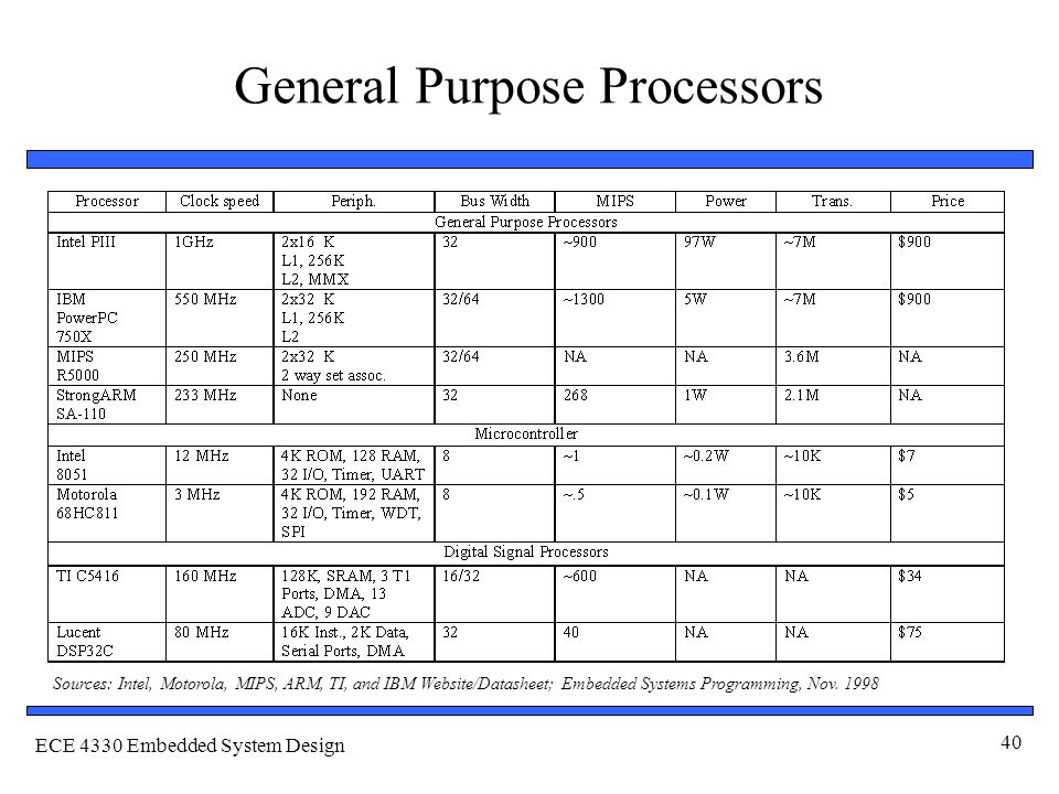
ECE 4330 Embedded System Design 40 General Purpose Processors Sources: Intel, Motorola, MIPS, ARM, TI, and IBM Website/Datasheet; Embedded Systems Programming, Nov. 1998
41
ECE 4330 Embedded System Design 41 Designing a General Purpose Processor Not something an embedded system designer normally would do –But instructive to see how simply we can build one top down –Remember that real processors aren’t usually built this way Much more optimized, much more bottom-up design Declarations: bit PC[16], IR[16]; bit M[64k][16], RF[16][16]; Aliases: op IR[15..12] rn IR[11..8] rm IR[7..4] dir IR[7..0] imm IR[7..0] rel IR[7..0] Reset Fetch Decode IR=M[PC]; PC=PC+1 Mov1 RF[rn] = M[dir] Mov2 Mov3 Mov4 Add Sub Jz 0110 0101 0100 0011 0010 0001 op = 0000 M[dir] = RF[rn] M[rn] = RF[rm] RF[rn]= imm RF[rn] =RF[rn]+RF[rm] RF[rn] = RF[rn]-RF[rm] PC=(RF[rn]=0) ?rel :PC to Fetch PC=0; from states below FSMD
![ECE 4330 Embedded System Design 41 Designing a General Purpose Processor Not something an embedded system designer normally would do –But instructive to see how simply we can build one top down –Remember that real processors aren’t usually built this way Much more optimized, much more bottom-up design Declarations: bit PC[16], IR[16]; bit M[64k][16], RF[16][16]; Aliases: op IR[15..12] rn IR[11..8] rm IR[7..4] dir IR[7..0] imm IR[7..0] rel IR[7..0] Reset Fetch Decode IR=M[PC]; PC=PC+1 Mov1 RF[rn] = M[dir] Mov2 Mov3 Mov4 Add Sub Jz op = 0000 M[dir] = RF[rn] M[rn] = RF[rm] RF[rn]= imm RF[rn] =RF[rn]+RF[rm] RF[rn] = RF[rn]-RF[rm] PC=(RF[rn]=0) rel :PC to Fetch PC=0; from states below FSMD](http://images.slideplayer.com/16/5148410/slides/slide_41.jpg "ECE 4330 Embedded System Design 41 Designing a General Purpose Processor Not something an embedded system designer normally would do –But instructive to see how simply we can build one top down –Remember that real processors aren’t usually built this way Much more optimized, much more bottom-up design Declarations: bit PC[16], IR[16]; bit M[64k][16], RF[16][16]; Aliases: op IR[15..12] rn IR[11..8] rm IR[7..4] dir IR[7..0] imm IR[7..0] rel IR[7..0] Reset Fetch Decode IR=M[PC]; PC=PC+1 Mov1 RF[rn] = M[dir] Mov2 Mov3 Mov4 Add Sub Jz op = 0000 M[dir] = RF[rn] M[rn] = RF[rm] RF[rn]= imm RF[rn] =RF[rn]+RF[rm] RF[rn] = RF[rn]-RF[rm] PC=(RF[rn]=0) rel :PC to Fetch PC=0; from states below FSMD")
42
ECE 4330 Embedded System Design 42 Architecture of a Simple Microprocessor Storage devices for each declared variable –register file holds each of the variables Functional units to carry out the FSMD operations –One ALU carries out every required operation Connections added among the components’ ports corresponding to the operations required by the FSM Unique identifiers created for every control signal Datapath IRPC Controller (Next-state and control logic; state register) Memory RF (16) RFwa RFwe RFr1a RFr1e RFr2a RFr2e RFr1RFr2 RFw ALU ALUs 2x1 mux ALUz RFs PCld PCinc PCclr 3x1 mux Ms MweMre To all input control signals From all output control signals Control unit 16 Irld 2 1 0 A D 1 0
 Memory RF (16) RFwa RFwe RFr1a RFr1e RFr2a RFr2e RFr1RFr2 RFw ALU ALUs 2x1 mux ALUz RFs PCld PCinc PCclr 3x1 mux Ms MweMre To all input control signals From all output control signals Control unit 16 Irld A D 1 0")
43
ECE 4330 Embedded System Design 43 A Simple Microprocessor FSM operations that replace the FSMD operations after a datapath is created RFwa=rn; RFwe=1; RFs=01; Ms=01; Mre=1; RFr1a=rn; RFr1e=1; Ms=01; Mwe=1; RFr1a=rn; RFr1e=1; Ms=10; Mwe=1; RFwa=rn; RFwe=1; RFs=10; RFwa=rn; RFwe=1; RFs=00; RFr1a=rn; RFr1e=1; RFr2a=rm; RFr2e=1; ALUs=00 RFwa=rn; RFwe=1; RFs=00; RFr1a=rn; RFr1e=1; RFr2a=rm; RFr2e=1; ALUs=01 PCld= ALUz; RFrla=rn; RFrle=1; MS=10; Irld=1; Mre=1; PCinc=1; PCclr=1; Reset Fetch Decode IR=M[PC]; PC=PC+1 Mov1 RF[rn] = M[dir] Mov2 Mov3 Mov4 Add Sub Jz 0110 0101 0100 0011 0010 0001 op = 0000 M[dir] = RF[rn] M[rn] = RF[rm] RF[rn]= imm RF[rn] =RF[rn]+RF[rm] RF[rn] = RF[rn]-RF[rm] PC=(RF[rn]=0) ?rel :PC to Fetch PC=0; from states below FSMD Datapath IRPC Controller (Next-state and control logic; state register) Memory RF (16) RFwa RFwe RFr1a RFr1e RFr2a RFr2e RFr1RFr2 RFw ALU ALUs 2x1 mux ALUz RFs PCld PCinc PCclr 3x1 mux Ms MweMre To all input contro l signals From all output control signals Control unit 16 Irld 2 1 0 A D 1 0 You just built a simple microprocessor!
![ECE 4330 Embedded System Design 43 A Simple Microprocessor FSM operations that replace the FSMD operations after a datapath is created RFwa=rn; RFwe=1; RFs=01; Ms=01; Mre=1; RFr1a=rn; RFr1e=1; Ms=01; Mwe=1; RFr1a=rn; RFr1e=1; Ms=10; Mwe=1; RFwa=rn; RFwe=1; RFs=10; RFwa=rn; RFwe=1; RFs=00; RFr1a=rn; RFr1e=1; RFr2a=rm; RFr2e=1; ALUs=00 RFwa=rn; RFwe=1; RFs=00; RFr1a=rn; RFr1e=1; RFr2a=rm; RFr2e=1; ALUs=01 PCld= ALUz; RFrla=rn; RFrle=1; MS=10; Irld=1; Mre=1; PCinc=1; PCclr=1; Reset Fetch Decode IR=M[PC]; PC=PC+1 Mov1 RF[rn] = M[dir] Mov2 Mov3 Mov4 Add Sub Jz op = 0000 M[dir] = RF[rn] M[rn] = RF[rm] RF[rn]= imm RF[rn] =RF[rn]+RF[rm] RF[rn] = RF[rn]-RF[rm] PC=(RF[rn]=0) rel :PC to Fetch PC=0; from states below FSMD Datapath IRPC Controller (Next-state and control logic; state register) Memory RF (16) RFwa RFwe RFr1a RFr1e RFr2a RFr2e RFr1RFr2 RFw ALU ALUs 2x1 mux ALUz RFs PCld PCinc PCclr 3x1 mux Ms MweMre To all input contro l signals From all output control signals Control unit 16 Irld A D 1 0 You just built a simple microprocessor!](http://images.slideplayer.com/16/5148410/slides/slide_43.jpg "ECE 4330 Embedded System Design 43 A Simple Microprocessor FSM operations that replace the FSMD operations after a datapath is created RFwa=rn; RFwe=1; RFs=01; Ms=01; Mre=1; RFr1a=rn; RFr1e=1; Ms=01; Mwe=1; RFr1a=rn; RFr1e=1; Ms=10; Mwe=1; RFwa=rn; RFwe=1; RFs=10; RFwa=rn; RFwe=1; RFs=00; RFr1a=rn; RFr1e=1; RFr2a=rm; RFr2e=1; ALUs=00 RFwa=rn; RFwe=1; RFs=00; RFr1a=rn; RFr1e=1; RFr2a=rm; RFr2e=1; ALUs=01 PCld= ALUz; RFrla=rn; RFrle=1; MS=10; Irld=1; Mre=1; PCinc=1; PCclr=1; Reset Fetch Decode IR=M[PC]; PC=PC+1 Mov1 RF[rn] = M[dir] Mov2 Mov3 Mov4 Add Sub Jz op = 0000 M[dir] = RF[rn] M[rn] = RF[rm] RF[rn]= imm RF[rn] =RF[rn]+RF[rm] RF[rn] = RF[rn]-RF[rm] PC=(RF[rn]=0) rel :PC to Fetch PC=0; from states below FSMD Datapath IRPC Controller (Next-state and control logic; state register) Memory RF (16) RFwa RFwe RFr1a RFr1e RFr2a RFr2e RFr1RFr2 RFw ALU ALUs 2x1 mux ALUz RFs PCld PCinc PCclr 3x1 mux Ms MweMre To all input contro l signals From all output control signals Control unit 16 Irld A D 1 0 You just built a simple microprocessor!")
44
ECE 4330 Embedded System Design 44 Chapter Summary General-purpose processors –Good performance, low NRE, flexible Controller, datapath, and memory Structured languages prevail –But some assembly level programming still necessary Many tools available –Including instruction-set simulators, and in-circuit emulators ASIPs –Microcontrollers, DSPs, network processors, more customized ASIPs Choosing among processors is an important step Designing a general-purpose processor is conceptually the same as designing a single-purpose processor

Similar presentations


 >")


 Development.>")
 Development.>")