Download presentation
Presentation is loading. Please wait.

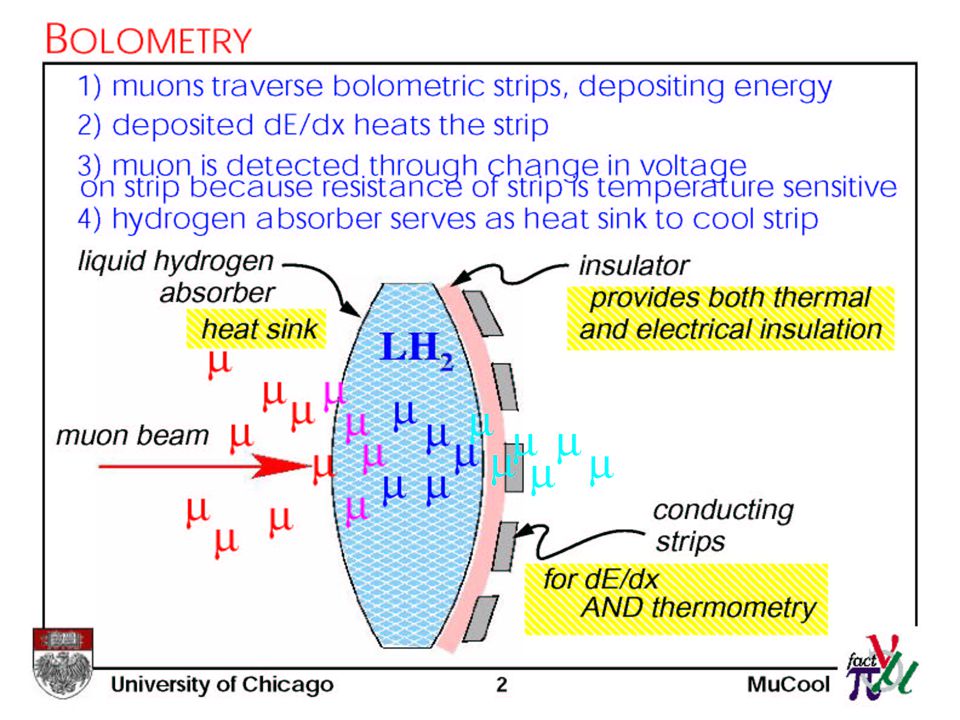
1
Kara Hoffman Mark Oreglia

3
A promising bolometric material: platinum high Z = large dE/dx temperature-resistivity function very steep at 20K should be more sensitive than the nickel and graphite prototypes previously tested in electron beams at Argonne Platinum TCR curve

4
0.30 - 0.35 K 0.25 - 0.30 0.20 - 0.25 0.10 - 0.15 0.15 - 0.20 0.00 - 0.05 0.05 - 0.10 2 beam radius Specific application: the linac test facility GEANT3 simulation Corresponding % resistivity change in bolometer strip

5
Bolometry summary Advantages: doesn’t disturb the beam relatively inexpensive robust Drawbacks: must be applied to absorber window for heat sinking – could be an issue mechanically/safetywise and cannot be removed or replaced small signal, particularly for more diffuse beams metal strips provide challenge in large electromagnetic noise environment large thermal time constants

6
Diamond is prized for more than just its sparkle (high refractive index)… low leakage I very fast readout no p-n junction needed low capacitance rad hard, strong no cooling hard insensitive to ’s >220nm Makes a great particle detector! The RD42 collaboration (CERN) has been developing diamond (primarily) as a microvertex detector.
 has been developing diamond (primarily) as a microvertex detector..")
7
- - - - + + + + diamond substrate ~300 m E (>1 V/ m) sputtered metal strips/pixels (titanium coated with gold) solid electrode Ionizing radiation (36 e-h pairs per m per mip) Anatomy of a diamond substrate microstrip detector… Essentially a very compact solid-state ionization chamber.
 sputtered metal strips/pixels (titanium coated with gold) solid electrode Ionizing radiation (36 e-h pairs per m per mip) Anatomy of a diamond substrate microstrip detector… Essentially a very compact solid-state ionization chamber.")
8
Polycrystalline CVD Diamond growth side substrate side induced charge: dx= distance e-holes drift apart = carrier mobility, = carrier lifetime Charge collection efficiency effected by: grain boundaries in grain defects

9
Can we read out both sides of the detector? E. Milani University of Rome Naïve answer is yes, however, holes are generally less mobile than electrons. Charge collection efficiency could be much lower. Efficiency may not be an issue in a high intensity beam. Diamond has been successfully implemented as a pixel detector, but that complicates DAQ. Could flip polarity and alternate coordinates, if necessary.

10
Radiation “Hardness” RD42 RD42 irradiation studies our linac GEANT3 Protons in Diamond RD42 has irradiated diamond to proton fluences of and they still function

11
Charge threshold above which 90% of events fall Annealing “Pumping” passivates traps, actually improving charge collection efficiency up to a fluence of Collected charge (e-) RD42 Initially, smaller signals become larger and response becomes more uniform.
 RD42 Initially, smaller signals become larger and response becomes more uniform.")
12
Electronics We have a 1 GHz bandwidth Tektronix oscilloscope with 400 ps rise time, 10 GS/s sample rate. Good enough? Power supply/amplifier: must maintain bias voltage while reading out a potentially large signal. High bandwidth: Fast electronics are desirable to exploit the excellent timing characteristics. Wide dynamic range: Large variation in intensities to be measured German nuclear scientists have developed such an amplifier DBA-II (Diamond Broadband Amplifier) – It can be done. Electronics is not a showstopper. Level of complexity depends on timing resolution desired.
 – It can be done. Electronics is not a showstopper. Level of complexity depends on timing resolution desired..")
13
A (Destructive) Test Open Questions Can we simultaneously read 2 coordinates from the same detector? How will they perform with such a large instantaneous particle flux? Will the response be linear or is there some saturation point? What kind of time resolution can we achieve? Quantify “ rad-hard ”. No one has irradiated them to a fluence where they had no signal. Place a small (1sq. cm) diamond detector with a single electrode on each side in a proton beam. Place a small (1sq. cm) diamond detector with a single electrode on each side in a proton beam. Monitor both electrodes and compare signal strength for electrons and holes. Monitor both electrodes and compare signal strength for electrons and holes. Continue until signal completely disappears. Continue until signal completely disappears. Remetalize electrodes and repeat process to determine whether the diamond is toast or the electrodes simply vaporized. Remetalize electrodes and repeat process to determine whether the diamond is toast or the electrodes simply vaporized.
 diamond detector with a single electrode on each side in a proton beam. Place a small (1sq. cm) diamond detector with a single electrode on each side in a proton beam. Monitor both electrodes and compare signal strength for electrons and holes. Monitor both electrodes and compare signal strength for electrons and holes. Continue until signal completely disappears. Continue until signal completely disappears. Remetalize electrodes and repeat process to determine whether the diamond is toast or the electrodes simply vaporized. Remetalize electrodes and repeat process to determine whether the diamond is toast or the electrodes simply vaporized..")
14
Potential advantages/payoffs sensitive (2 coordinate?) measurement relatively huge signal fast (subnanosecond ~40ps) response might allow temporal beam profiling, in addition to current and position measurements free standing-accessible low Z- no beam loss (<0.1%) could be implemented quickly RD42 has already developed a vendor (DeBeers) could have broader applications: for other beams – single particle efficiency, high bandwidth make it suitable for transfer lines, etc. measuring Lab G “ death rays ” and other RF cavities

15
Now back to the linac test facility… Ed Black and I have sketched a robotic arm to sweep the diamond sensor through the beam Allows us to pull sensor out of the beam, thus increasing sensor life by minimizing radiation exposure. A single sensor can be used to sample the beam at several different radii, thus minimizing cost while still allowing us to make a full 3 measurement.

16
Diamond quality: cut, clarity = COST! Size of single crystals Density of traps Purity Polishing Uniformity of thickness and response Industrial diamond is manufactured primary for heat sinking or optics. For HEP, the figure of merit is charge collection distance. Price range: Electronics grade (P1 diamond, and others) ~$100/cm2 Tracking grade (DeBeers only) >>$1000/cm2 We don’t need single particle efficiency to see a beam. “Crappy” diamond will probably work.
 ~$100/cm2 Tracking grade (DeBeers only) >>$1000/cm2 We don’t need single particle efficiency to see a beam. Crappy diamond will probably work..")
17
Needs?$ ComponentSupplierCost 2 CVD diamond wafers: 5x5 cm each DeBeers Industrial (via U. of Toronto) Waiting for a quote from W. Trischuk 8 mm x 8 mm diamond square P1 Diamond$150 - cost goes down with volume Metal lead sputtering Rutgers U.<$300 data acquisition electronics U. Chicago- We probably don’t need this quality.
 Waiting for a quote from W. Trischuk 8 mm x 8 mm diamond square P1 Diamond$150 - cost goes down with volume Metal lead sputtering Rutgers U.<$300 data acquisition electronics U. Chicago- We probably don’t need this quality..")
18
I am negotiating with RD42 to borrow/purchase a 1 sq. cm piece of “tracking grade” diamond, and I’m purchasing some electronics grade diamond for destructive test. I believe we can “beam test” (or nuke rather) some samples on a short time scale. If “electronics grade” stuff works, it could be “disposable”. This talk probably no longer belongs in an absorber review.
 some samples on a short time scale. If electronics grade stuff works, it could be disposable . This talk probably no longer belongs in an absorber review..")
19
Extra slide: comparison of physical properties of polycrystalline and single crystal diamond

Similar presentations


: Diamond Beam Monitor (DBM) News from two diamond manufacturers.>")


