Download presentation
Presentation is loading. Please wait.

1
Characterisation and Reliability testing of THz Schottky diodes. By Chris Price C.M.Price@rl.ac.uk Supervisor: Dr Byron Alderman December 2006 Preliminary Presentation

2
Contents Problems with THz technology What is a Schottky diode What are Schottky diodes used for The fabrication method European situation Characterisation Reliability Summarise current position Future plans Questions ??? Probe station (Pegasus s200)
.")
3
Problems with THz Technology THz frequencies are loosely defined in the range of 0.1-10 THz There is an absence of low cost, miniaturised solid state power supplies 10 -3 10 -2 10 -1 110 Frequency (THz)
")
4
Problems with THz Technology Transit Time Devices (up to 170 GHz) Advanced electronics Equivalent to commercially available devices with reduced dimensions Maximum frequency determined by; Time taken for a carrier to move a characteristic distance And to a lesser extent the RC time constant
 Advanced electronics Equivalent to commercially available devices with reduced dimensions Maximum frequency determined by; Time taken for a carrier to move a characteristic distance And to a lesser extent the RC time constant")
5
Problems with THz Technology Energy Transition Devices –Charge carriers undergo a transition between energy states –Frequency given by (E 2 – E 1 )= h f Problems; –Cannot get population inversion at room temperatures –Photon density of states α Frequency^2 E2E2 E1E1 Photon Frequency, f
= h f Problems; –Cannot get population inversion at room temperatures –Photon density of states α Frequency^2 E2E2 E1E1 Photon Frequency, f")
6
Recombination of electrons and holes occurs creating a depletion zone What is a Schottky diode P-N diode is a combination to two oppositely doped semi-conductors P- TypeN- Type Energy Band diagram of P-N junction

7
What is a Schottky diode Combination of metal and a semi-conductor This creates; –Lower junction voltage –Almost non-existent depletion width in metal Another property of Schottky diodes; –Majority carrier No slow random recombination Energy band diagram of Schottky junction

8
Planar Schottky diode Air Bridge Schottky Contact Ohmic Diode current voltage relationship is given by; i is the current I 0 is reverse saturation current q is the charge on an electron V d is voltage across the diode k b is the Boltzmann constant T is the temperature in kelvin η is the ideality

9
What diodes are used for Two devices that use the non-linear properties are; Multipliers (diode used as a varactor) –High frequency multipliers use the nonlinear capacitance property, and a filter to eliminate specific harmonics and produce an output that is a multiple of the input frequency
 –High frequency multipliers use the nonlinear capacitance property, and a filter to eliminate specific harmonics and produce an output that is a multiple of the input frequency")
10
Mixers (diode used as a varistor) A mixer is a non linear circuit that receives two input signals and outputs a signal equal to the difference and to the sum of the two input frequencies What diodes are used for
 A mixer is a non linear circuit that receives two input signals and outputs a signal equal to the difference and to the sum of the two input frequencies What diodes are used for")
11
The creation of these diodes can be broken down into four stages: 1)Making the ohmic 2)Making the Schottky contact 3)Making the finger 4)Making the air gap 1 2 3 41 2 3 4 Fabrication Process
Making the ohmic 2)Making the Schottky contact 3)Making the finger 4)Making the air gap Fabrication Process")
12
Preparing the ohmic Annealer Thermal evaporator

13
Schottky Contact E- beam evaporator

14
Anode Finger

15
Air Gap

16
Virginia Diodes Inc. (VDI) –Leading supplier of Schottky diodes –Concerns over future availability University of Bath –Made limited progress Darmstadt –Are developing a novel approach UMS –Provide commercial diodes, but no influence over design RAL –Produced leading mixer results at 200 GHz –Very much at the forefront of technology Supply Situation in Europe
 –Leading supplier of Schottky diodes –Concerns over future availability University of Bath –Made limited progress Darmstadt –Are developing a novel approach UMS –Provide commercial diodes, but no influence over design RAL –Produced leading mixer results at 200 GHz –Very much at the forefront of technology Supply Situation in Europe.")
17
Two methods: –Current Voltage (IV) Measures DC characteristics Useful for mixers –Capacitance Voltage (CV) Measures AC characteristics Useful for multipliers Probe station (Pegasus S200) Characterisation
 Measures DC characteristics Useful for mixers –Capacitance Voltage (CV) Measures AC characteristics Useful for multipliers Probe station (Pegasus S200) Characterisation")
18
IV setup Basic Circuit

19
Calculating Parameters Parameters Interested in; –Spreading Resistance R s, –Ideality η and –Reverse saturation current I 0 Two methods of calculations: –Standard formulae on current point measurements –Curve fitting the IV characteristics at arbitrary measurement points

20
Calculating Parameters Standard formula ΔV = V 3 – V 4 R s = 1000 ((V 5 – V 4 ) – ΔV η = q ΔV log 10 (e) / (k B T) I 0 = i 1 / (exp ((q V 1 ) /(η k B T)) – 1) Allows comparison between measurements Good heritage for comparisons with previously used diodes but If two or more points are missed comparison is no longer valid
 – ΔV η = q ΔV log 10 (e) / (k B T) I 0 = i 1 / (exp ((q V 1 ) /(η k B T)) – 1) Allows comparison between measurements Good heritage for comparisons with previously used diodes but If two or more points are missed comparison is no longer valid")
21
Curve fitting –Derived from IV equation and –assumes there is a constant spreading resistance also –Assuming that i >> I 0 –Substituting in V d = V – i R s –V = a ln(i) + b i + c –Least square fits is performed to calculate the coefficients Calculating Parameters
 + b i + c –Least square fits is performed to calculate the coefficients Calculating Parameters")
22
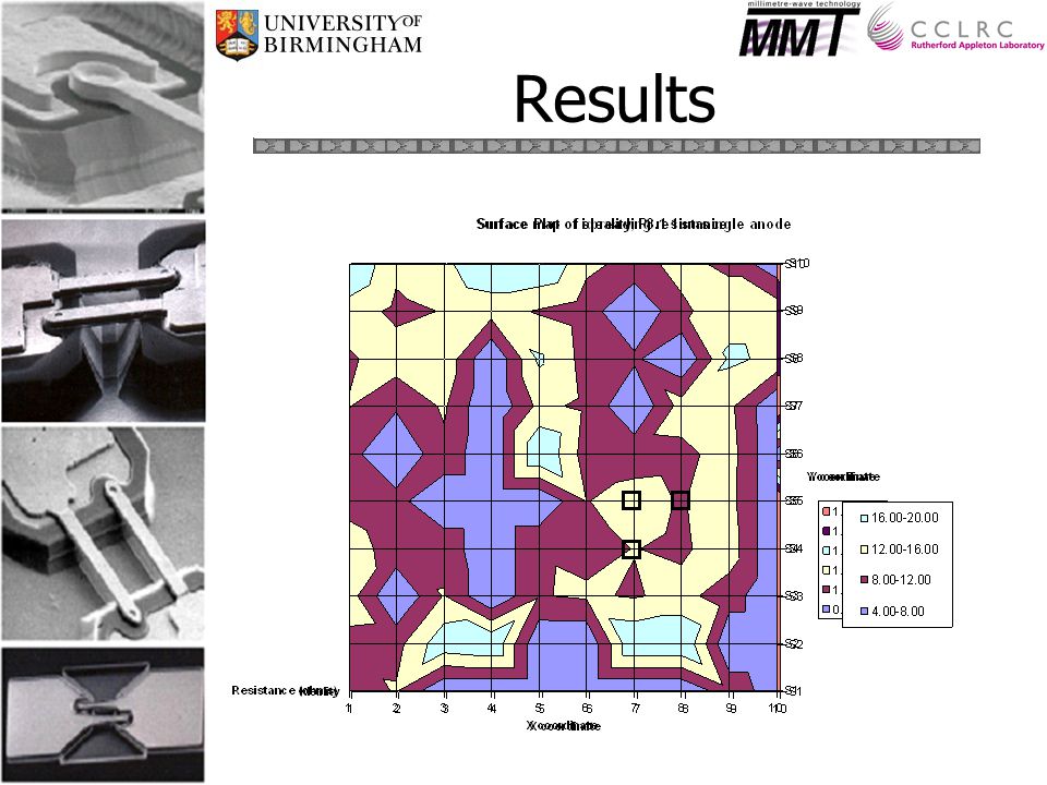
Results

24
Scanning electron microscope (SEM) IV setup Problem;
 IV setup Problem;")
25
Reliability Tests Defined as how resistant it is to failure Failure criteria; –A 10% deviation from original measurements. Simple tests –Repeatability –Soldering –Thermal Cycling Accelerated Life tests –Thermal –Humidity –Electrical Biasing

26
Summary Current Situation: –Understood how the IV characterisation calculations are done and –how the Probe Station works –I have separated the diodes and currently building the basic circuit for the reliability tests and –I am currently learning LabView Above: Diced diode from a wafer Left: dicing saw

27
Future plans Remove bugs from the probe station and calibrate with new heads Develop the software necessary Build thermal experiment Perform repeatability test Perform soldering test Analyse data collected

28
Any Questions ???

Similar presentations


>")


>")


