Download presentation
Presentation is loading. Please wait.

1
Micromachining of Silicon and Its Applications in MEMS and Intelligent Sensors Mustafa G. Guvench, Ph.D. University of Southern Maine

2
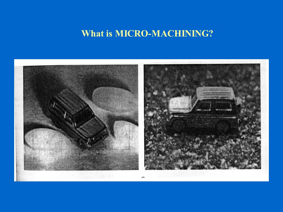
What is MICRO-MACHINING?

6
What can Micromachined Parts/Systems do for us? Be a Conduit to Microscopic Domain: 1. Sensing (Information) 2. Information Processing 3. Communication 4. Manipulation (Actuation and Control)
 2. Information Processing 3. Communication 4. Manipulation (Actuation and Control).")
7
Why / Why not SILICON? Semiconductor: Active Devices + Sensors (Photo-Magneto-Strain Sensing) Insulator:SiO 2, Si 3 N 4, Glass Thin Film Conductor:Aluminum, Gold, Silicides PhotoLithography:Planar control (+ & -)
 Insulator:SiO 2, Si 3 N 4, Glass Thin Film Conductor:Aluminum, Gold, Silicides PhotoLithography:Planar control (+ & -).")
8
Mechanical Material SILICON? Stiff => Thinning is required for appreciable strain

9
Micromachining of SILICON? MICROMACHINING of SILICON => (a) BULK (substrate) (b) SURFACE (films) Additive Processes: Chemical and Physical Deposition (Thin Layers only) (Single/Poly) Removal Processes:Chemical and Physical Etching (Wet/Dry/Plasma/Inert/Reactive) (Bulk/Film) (Anisotropic/Isotropic) (Bulk/Film) (Anisotropic/Isotropic)
 BULK (substrate) (b) SURFACE (films) Additive Processes: Chemical and Physical Deposition (Thin Layers only) (Single/Poly) Removal Processes:Chemical and Physical Etching (Wet/Dry/Plasma/Inert/Reactive) (Bulk/Film) (Anisotropic/Isotropic) (Bulk/Film) (Anisotropic/Isotropic).")
10
BULK MICROMACHINING (Etchants: Isotropic/Anisotropic)
")
11
BULK MICROMACHINING (Isotropic/Anisotropic)
")
12
BULK MICROMACHINING (Cavity/Cantilever Anisotropic)
")
13
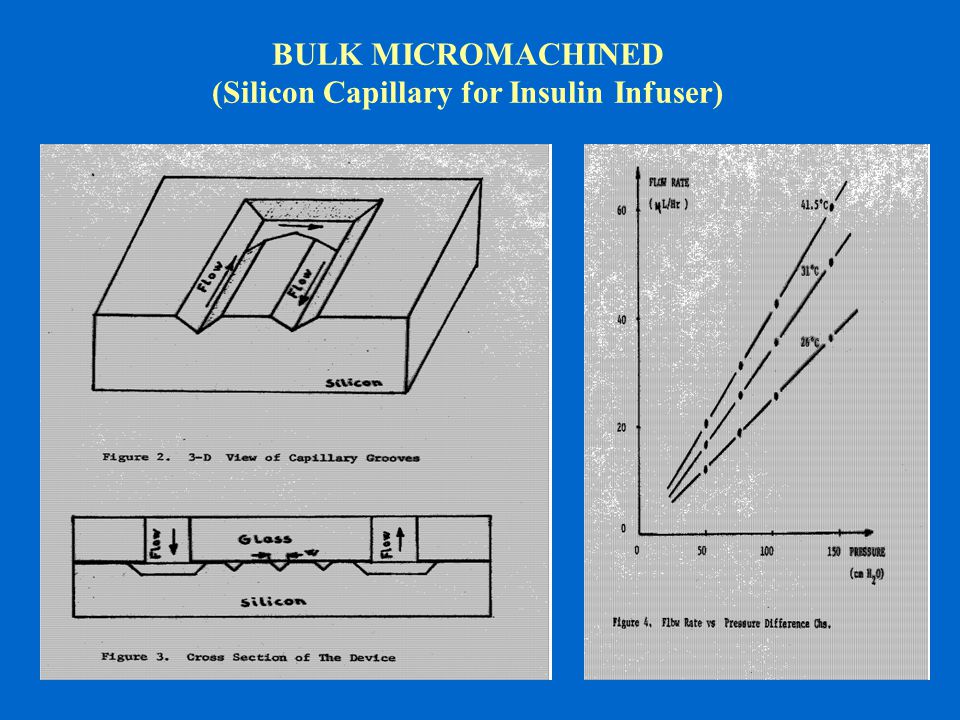
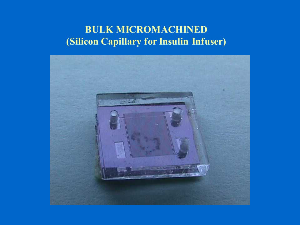
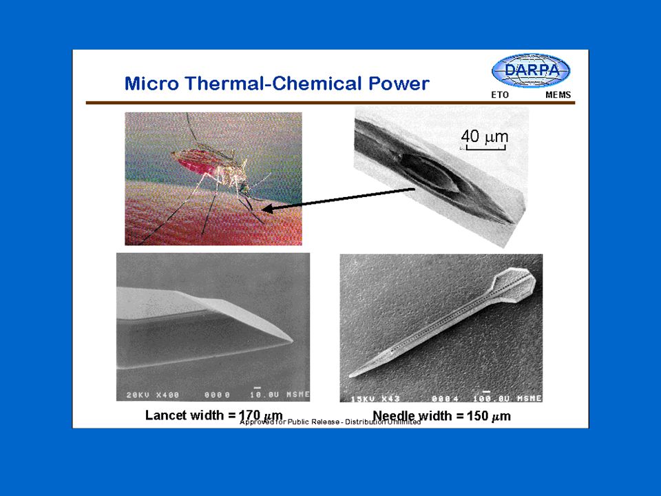
BULK MICROMACHINED (Silicon Capillary for Insulin Infuser)
")
16
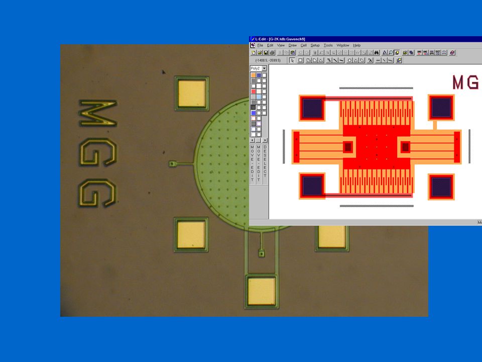
BULK MICROMACHINED (Silicon Mask for Cylindrical Micromotion Sensor)
")
17
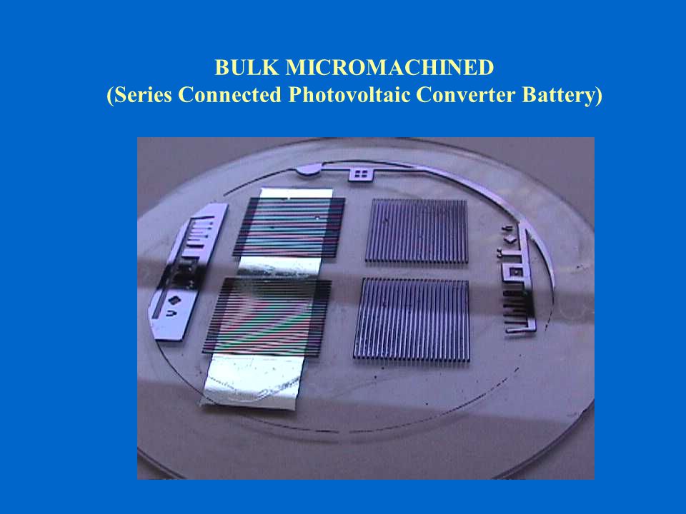
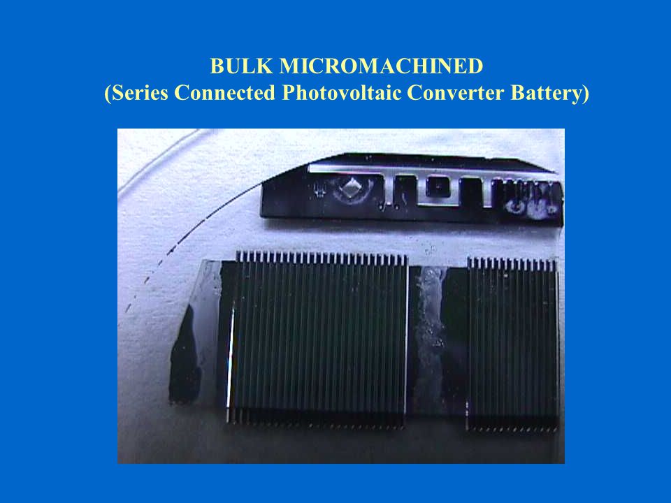
BULK MICROMACHINED (Series Connected Photovoltaic Converter Battery)
")
21
MOTION? HANDLING? ASSEMBLY?COUPLING? =>

22
Micro Electro Mechanical Sytems

24
M (CMOS-IC Technology) + E (CMOS-IC Technology) + M (Silicon and Sacrificial Layers) + O (Aluminum) + S (IC Packaging Technology)
 + E (CMOS-IC Technology) + M (Silicon and Sacrificial Layers) + O (Aluminum) + S (IC Packaging Technology)")
25
Three-Layer Poly-Silicon Surface Micromachining Process (to build Mechanical Parts on CMOS IC) Final cross sectional view with 7 layers
 Final cross sectional view with 7 layers")
26
Three-Layer Poly-Silicon Surface Micromachining Process

27
Surface Micromachined

28
Micromachining of Projection Camera

30
M (CMOS-IC Technology) + E (CMOS-IC Technology) + M (Silicon and Sacrificial Layers) + O (Aluminum) + S (IC Packaging Technology) M.G.Guvench
 + E (CMOS-IC Technology) + M (Silicon and Sacrificial Layers) + O (Aluminum) + S (IC Packaging Technology) M.G.Guvench")
31
Surface Micromachined Silicon Sensors M.G.Guvench

32
M.G.Guvench

33
Electrostatic Field Sensors M.G.Guvench

34
M.G.Guvench

35
M.G.Guvench

36
Mass (Absorption/Deposition) Sensor M.G.Guvench
 Sensor M.G.Guvench")
37
M.G.Guvench

38
M.G.Guvench

39
Electrostatic Field Sensors M.G.Guvench

40
Flow Skin Friction Sensors M.G.Guvench

41
M.G.Guvench

42
CMOS Analog Chip Design (Operational Amplifier) M.G.Guvench
 M.G.Guvench")
43
MicroFab Laboratory

44
Programmable Diffusion/Oxidation System’s Controller in The MicroFab Laboratory

45
Double-Diffused P + NN + Junction PhotoDiode Made Being Tested in The MicroFabrication Lab.

46
MicroFab Laboratory

47
Surface Micromachined Silicon Sensors M.G.Guvench

48
3-Poly Surface Micromachining Processed Sensors Cross Section

50
MEMS Switch

51
MEMS Micromotor

52
A Mass (Absorption/Deposition) Sensor M.G.Guvench
 Sensor M.G.Guvench")
Similar presentations


>")


>")


