Download presentation
Presentation is loading. Please wait.

1
Ideal Diode Equation

2
Topics of This Lecture Ideal Diode Equation Its origins
Current versus Voltage (I-V) characteristics How to calculate the magnitude of the variables in the equation using real data What the limitations of this equation are How it is used in PSpice simulations
 characteristics. How to calculate the magnitude of the variables in the equation using real data. What the limitations of this equation are. How it is used in PSpice simulations.")
3
P-N junctions The voltage developed across a p-n junction caused by
the diffusion of electrons from the n-side of the junction into the p-side and the diffusion of holes from the p-side of the junction into the n-side

4
Built-in Voltage This built-in voltage prevents all of the electrons and holes from diffusing throughout the diode until there is a constant concentration of electrons and holes everywhere (which would mean we would no longer have a diode).
.")
5
Reminder Drift currents only flow when there is an electric field present. Diffusion currents only flow when there is a concentration difference for either the electrons or holes (or both).
.")
7
Symbol for Diode

8
Biasing a Diode When Va > 0V, the diode is forward biased
When Va < 0V, the diode is reverse biased

9
When the applied voltage (Va) is zero
The diode voltage and current are equal to zero on average Any electron that diffuses through the depletion region from the n-side to the p-side is counterbalanced by an electron that drifts from the p-side to the n-side Any hole that diffuses through the depletion region from the p-side to the n-side is counterbalanced by an hole that drifts from the n-side to the p-side So, at any one instant (well under a nanosecond), we may measure a diode current. This current gives rise to one of the sources of electronic noise.
, we may measure a diode current. This current gives rise to one of the sources of electronic noise.")
10
Schematically Movement of electrons is noted in red; movement of holes is in blue. Modified from B. Van Zeghbroech, Principles of Semiconductor Devices

11
Applied voltage is less than zero
The energy barrier between the p-side and n-side of the diode became larger. It becomes less favorable for diffusion currents to flow It become more favorable for drift currents to flow The diode current is non-zero The amount of current that flows across the p-n junction depends on the number of electrons in the p-type material and the number of holes in the n-type material Therefore, the more heavily doped the p-n junction is the smaller the current will be that flows when the diode is reverse biased The applied voltage is always referenced in terms of the voltage applied to the p-side of the diode when the n-side of the diode is held at ground. Reverse biased means that the calculation of the voltage applied to the p-side of the diode minus the voltage applied to the n-side of the diode results in a negative number.

12
Schematically Modified from B. Van Zeghbroech, Principles of Semiconductor Devices

13
Plot of I-V of Diode with Small Negative Applied Voltage

14
Applied Voltage is greater than zero
The energy barrier between the p-side and n-side of the diode became smaller with increasing positive applied voltage until there is no barrier left. It becomes less favorable for drift currents to flow There is no electric field left to force them to flow There is nothing to prevent the diffusion currents to flow The diode current is non-zero The amount of current that flows across the p-n junction depends on the gradient of electrons (difference in the concentration) between the n- and p-type material and the gradient of holes between the p- and n-type material The point at which the barrier becomes zero (the flat-band condition) depends on the value of the built-in voltage. The larger the built-in voltage, the more applied voltage is needed to remove the barrier. It takes more applied voltage to get current to flow for a heavily doped p-n junction
 between the n- and p-type material and the gradient of holes between the p- and n-type material. The point at which the barrier becomes zero (the flat-band condition) depends on the value of the built-in voltage. The larger the built-in voltage, the more applied voltage is needed to remove the barrier. It takes more applied voltage to get current to flow for a heavily doped p-n junction.")
15
Schematically Modified from B. Van Zeghbroech, Principles of Semiconductor Devices

16
Plot of I-V of Diode with Small Positive Applied Voltage

17
Ideal Diode Equation Empirical fit for both the negative and positive I-V of a diode when the magnitude of the applied voltage is reasonably small.

18
Ideal Diode Equation Where
ID and VD are the diode current and voltage, respectively q is the charge on the electron n is the ideality factor: n = 1 for indirect semiconductors (Si, Ge, etc.) n = 2 for direct semiconductors (GaAs, InP, etc.) k is Boltzmann’s constant T is temperature in Kelvin kT/q is also known as Vth, the thermal voltage. At 300K (room temperature), kT/q = 25.9mV
 n = 2 for direct semiconductors (GaAs, InP, etc.) k is Boltzmann’s constant. T is temperature in Kelvin. kT/q is also known as Vth, the thermal voltage. At 300K (room temperature), kT/q = 25.9mV.")
19
Simplification When VD is negative When VD is positive

20
To Find n and IS Using the curve tracer, collect the I-V of a diode under small positive bias voltages Plot the I-V as a semi-log The y-intercept is equal to the natural log of the reverse saturation current The slope of the line is proportional to 1/n

21
Example

22
Questions How does the I-V characteristic of a heavily doped diode differ from that of a lightly doped diode? Why does the I-V characteristics differ? For any diode, how does the I-V characteristic change as temperature increases? For the same doping concentration, how does the I-V characteristic of a wide bandgap (EG) semiconductor compare to a narrow bandgap semiconductor (say GaAs vs. Si)? Look at what carriers are moving in the forward and reverse bias conditions and then think about the equation for the intrinsic carrier concentration.
 semiconductor compare to a narrow bandgap semiconductor (say GaAs vs. Si) Look at what carriers are moving in the forward and reverse bias conditions and then think about the equation for the intrinsic carrier concentration.")
23
What the Ideal Diode Equation Doesn’t Explain
I-V characteristics under large forward and reverse bias conditions Large current flow when at a large negative voltage (Breakdown voltage, VBR) ‘Linear’ relationship between ID and VD at reasonably large positive voltages (Va > ff)
 ‘Linear’ relationship between ID and VD at reasonably large positive voltages (Va > ff)")
24
VBR or VZ Slope = 1/RS Slope = 1/rz Von

25
Nonideal (but real) I-V Characteristic
Need another model Modifications to Ideal Diode Equation are used in PSpice We will see this in the list of parameters in the device model We will use a different model It is called the Piecewise Model

26
PSpice Simplest diode model in PSpice uses only the ideal diode equation More complex diode models in PSpice include: Parasitic resistances to account for the linear regions Breakdown voltage with current multipliers to map the knee between Io and the current at breakdown Temperature dependences of various parameters Parasitic capacitances to account for the frequency dependence

27
Capture versus Schematics
It doesn’t matter to me which you use I find Schematics easier, but the lab encourages the use of Capture

28
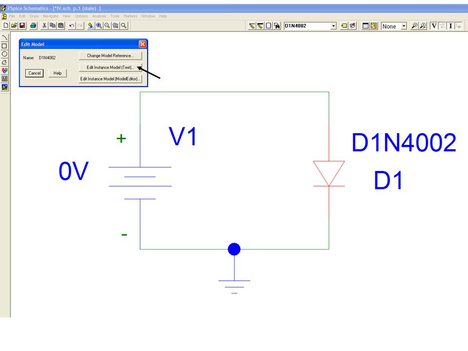
PSpice Schematics

29
To plot the I-V characteristics of the diode in PSpice, I run a DC sweep on this very simple circuit.

32
Device Parameters *** Power Diode *** Type of Diode .MODEL D1N4002-X D
Part Number ( IS=14.11E-9 Reverse Saturation Current N=1.984 Ideality Factor RS=33.89E-3 Forward Series Resistance IKF=94.81 High-Level Injection Knee Current in Forward Bias XTI=3 Temperature Dependence of Reverse Saturation Current EG=1.110 Energy Bandgap of Si CJO=51.17E-12 Junction Capacitance at Zero Applied Bias M=.2762 Grading Coefficient Inversely Proportional to Zener Resistance VJ=.3905 Turn-on Voltage FC=.5 Coefficient Associated with Forward Bias Capacitance ISR=100.0E-12 Reverse Saturation Current During Reverse Bias NR=2 Ideality Factor During Reverse Bias BV=100.1 Breakdown Voltage IBV=10 Current at Breakdown Voltage TT=4.761E-6 ) Transit Time of Carriers Across p-n Juntion
 Transit Time of Carriers Across p-n Juntion.")
33
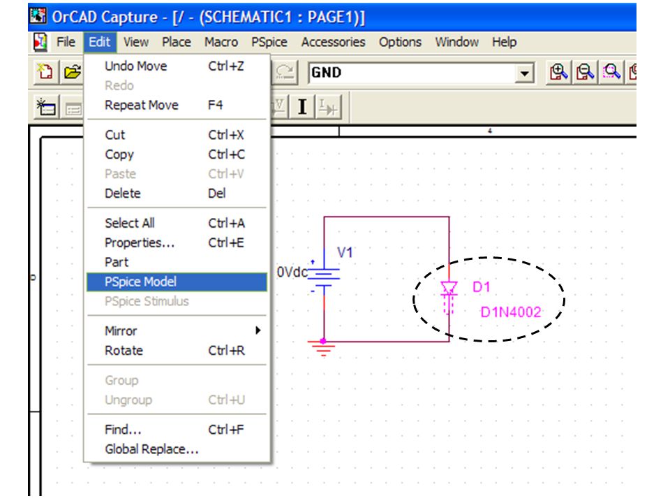
PSpice Capture

36
Editing Device Model The device parameters can be changed, but will only be changes for the file that you are currently working on. In Schematics, the changes only apply to the specific part that you had highlighted when you made the changes. In Capture, the changes apply to all components in the file that share the same part model. To simulate the Ideal Diode Equation, you can delete the other parameters or set them to zero or a very large number, depending on what would be appropriate to remove their effect from the simulation

37
Important Points of This Lecture
There are several different techniques that can be used to determine the diode voltage and current in a circuit Ideal diode equation Results are acceptable when voltages applied to diode are comparable or smaller than the turn-on voltage and more positive than about 75-90% of the breakdown voltage Piecewise model Results are acceptable when voltage applied to the diode are large in magnitude when comparable to the turn-on voltage and the breakdown voltage. 37

38
Embedded in the Ideal Diode Equation are dependences on
Temperature Doping concentration of p and n sides Semiconductor material Bandgap energy Direct vs. indirect bandgap PSpice diode model using Ideal Diode Eq. User can edit diode model Diode model can also be more complex to include deviations from Ideal Diode Eq. such as frequency dependence of operation 38

Similar presentations


>")


 – Carrier drift and diffusion PN Junction.>")